
Voltage Multiplier

A voltage multiplier circuit is designed to increase the voltage level of an input signal, typically a square wave, by utilizing capacitors and diodes to achieve the desired output. In this specific configuration, the circuit doubles the amplitude of the input square wave. The basic operation involves charging capacitors during one half of the waveform and discharging them to the load during the other half.
The circuit typically consists of a series of diodes and capacitors arranged in a specific topology. For instance, in a simple two-stage voltage doubler, the first diode allows current to flow into the capacitor during the positive half-cycle of the input waveform, charging it to the peak voltage minus the forward voltage drop of the diode. During the negative half-cycle, the charged capacitor discharges through the load, effectively doubling the output voltage.
It is important to note that there is a voltage drop associated with the base-emitter junction of transistors present in the circuit. This drop is typically around 2V, which must be accounted for in the design to ensure that the output voltage meets the required specifications. The overall efficiency of the circuit can be affected by these losses, and careful selection of components can help mitigate them.
Additional considerations for optimizing performance include selecting diodes with low forward voltage drops and capacitors with appropriate voltage ratings to handle the increased output voltage. The load connected to the output should also be considered, as it will influence the overall behavior of the circuit and its ability to maintain the desired output voltage under varying conditions. Proper thermal management may also be necessary to ensure reliability and longevity of the components used in the circuit.This is a voltage multiplier circuit. First circuit is used to double the a square wave (any amplitude). However there is minus about 2v losses in base-emitter.. 🔗 External reference
Related Circuits
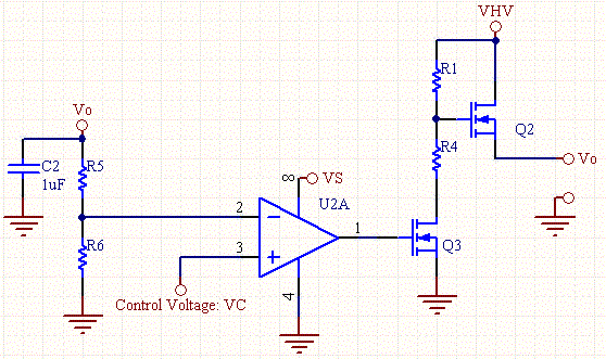
The drawback of the circuit mentioned is that the operational amplifier (op-amp) supply is connected to the high voltage (HV) supply. Most op-amps are limited to approximately 30V for their supply voltage, which prevents the circuit from functioning with...

This circuit is a DC to DC inverter that can convert a 12V DC battery voltage to a high voltage of 300V DC. This circuit operates with low current. This DC to DC inverter circuit is designed to efficiently step...
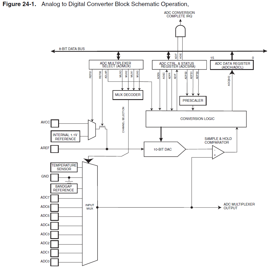
When using the internal 1.1V reference for the ADC, if the analog input exceeds 1.1V, such as 2.5V, it will not harm the microcontroller. Instead, the ADC value will clip at 0x3FF. Based on practical experience, it has been...
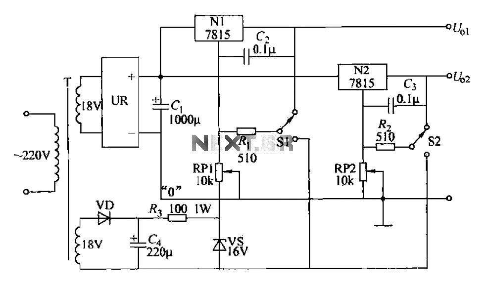
An adjustable dual voltage power supply circuit is presented, suitable for frequent experimental use. The current output does not exceed 1A, and both voltage outputs are adjustable. The circuit utilizes N1, N2, and 78 series three-terminal voltage regulator integrated...
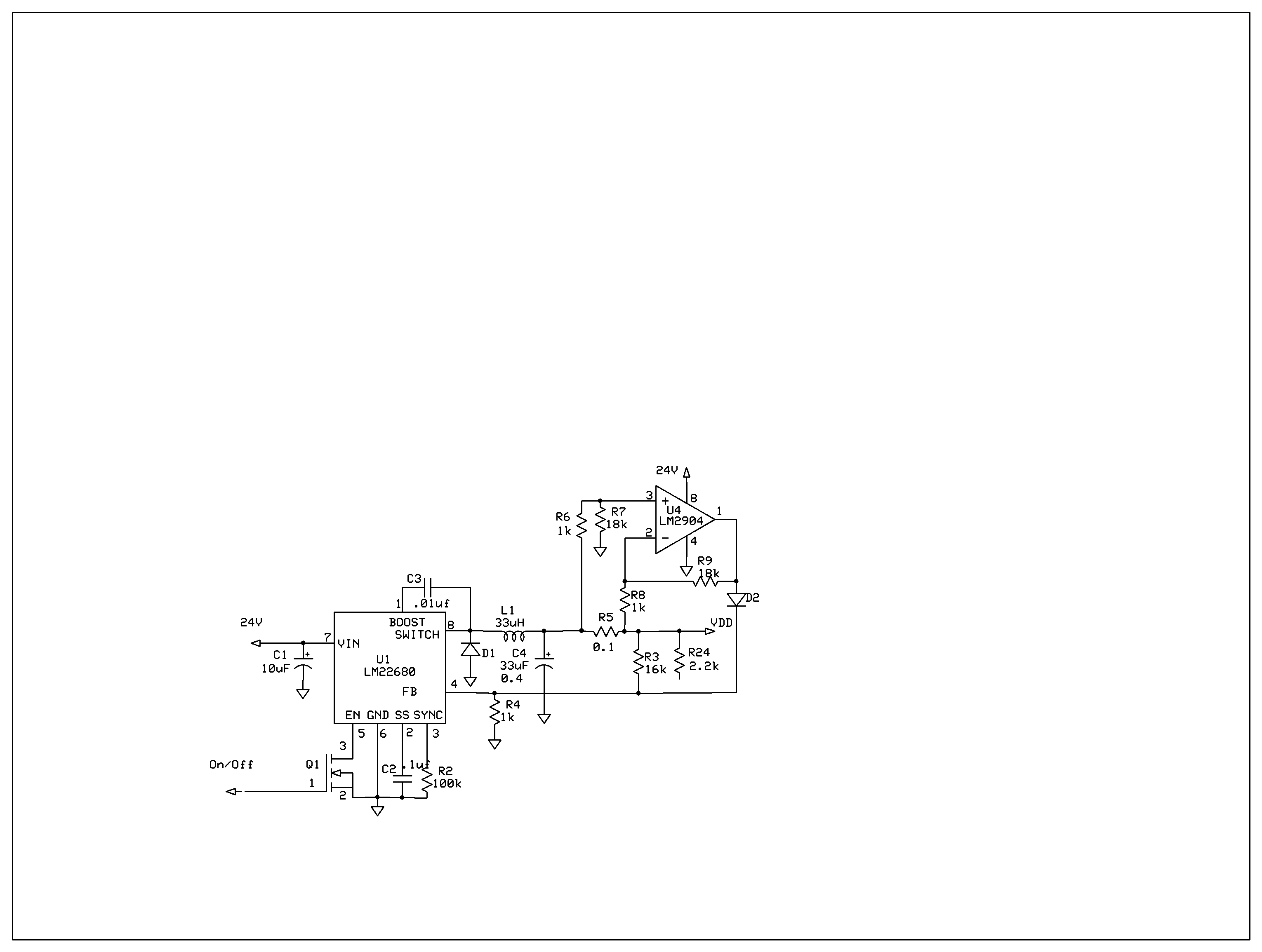
The product requires a voltage-controlled, current-limited power supply. Various switcher chips have been used with an op-amp to provide feedback for a current sense voltage to the feedback pin. Currently, an LM22680 is in use, but it has shown...
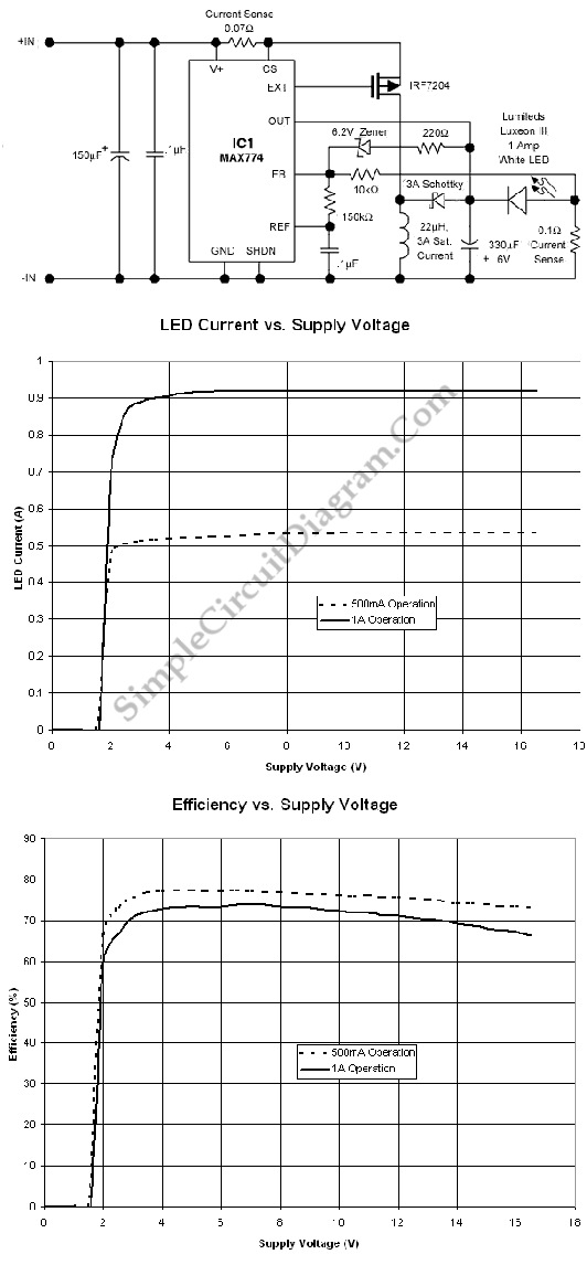
This is a high-power LED driver circuit designed to accommodate a wide input-voltage range. The circuit utilizes a buck/boost converter controller to regulate the current supplied to a white LED. The high-power LED driver circuit is engineered to effectively manage...