
Synchronous RS flip-flop circuit structure and symbols
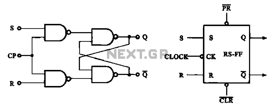
The synchronous RS flip-flop is a fundamental building block in digital electronics, providing a means to store a single bit of data while being controlled by a clock signal. This configuration helps eliminate the race conditions and unstable states that can occur in asynchronous designs.
The circuit is typically composed of two NAND gates configured as a bistable multivibrator. The inputs are designated as R (reset) and S (set), which control the state of the flip-flop. The addition of the clock input (CP) ensures that changes in the output state occur only on a specific edge of the clock signal, typically the rising edge.
When the clock input is high, the states of the R and S inputs are evaluated. If S is high and R is low, the output Q will be set to high (1), indicating that the flip-flop is in the set state. Conversely, if R is high and S is low, the output Q will be reset to low (0), indicating that the flip-flop is in the reset state. If both inputs are low, the output retains its previous state, demonstrating the memory characteristic of the flip-flop.
The circuit symbol for the synchronous RS flip-flop typically includes the two input terminals (S and R), the clock input (CP), and the output terminal (Q). The design ensures that the output only changes when the clock signal transitions, facilitating reliable timing and control in sequential circuits.
Overall, the synchronous RS flip-flop is essential for applications requiring precise timing and control in digital systems, such as counters, registers, and memory units. Its ability to synchronize with a clock signal allows for more predictable behavior in complex circuits.Aforementioned asynchronous RS flip-flop is not synchronized with the system clock signal synchronous RS flip-flop is the addition of the synchronization can be synchronized wi th the clock signal work. Figure (a) shows the circuit configuration of synchronous RS flip-flop, it will use two inputs, two NAND gates, and adds a clock input (CP), the circuit symbol shown in Figure (b), show
Related Circuits
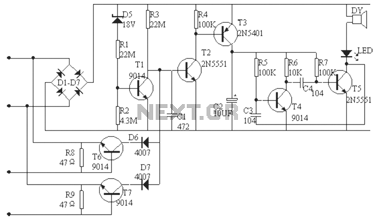
The phone alarm device is designed to monitor and prevent unauthorized use of a telephone line. When interference signals are detected on the line due to theft attempts, the alarm activates, preventing the thief from making calls while alerting...
The circuit can incorporate a buffer gate at the input to ensure compatibility with TTL or other logic levels. This design is intended for a TTL 0V circuit to accommodate a 3.5V input signal swing. Additionally, it generates a...
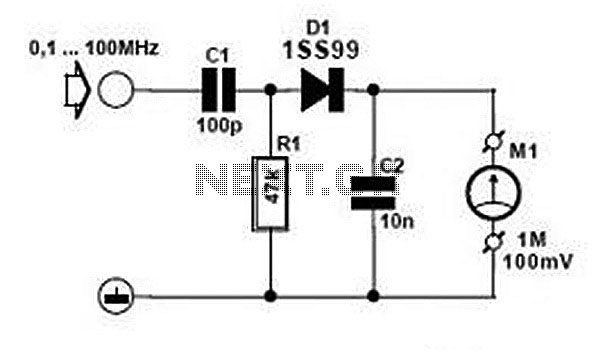
Comprehensive information about RF Probe Circuits is available. Users can learn about and download RF Probe Circuit designs online. RF Probe Circuits are essential tools for testing and analyzing radio frequency signals in various applications, including telecommunications, broadcasting, and electronic...
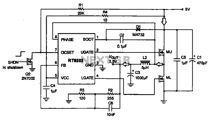
A 5V to 2.5V voltage regulator circuit is designed for use in computer motherboards. At its core, this circuit utilizes the RT9202 power management chip. The RT9202 functions as a switching pulse generating circuit, which, upon startup, converts a...
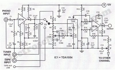
This Hi-Fi stereo preamplifier circuit is constructed using the TDA1054 integrated circuit (IC) from SGS. The TDA1054 is housed in a 16-pin DIL package and incorporates two separate preamplifier circuits. It is characterized by low noise and minimal issues...
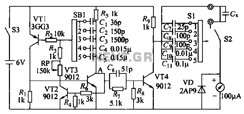
A capacitive measuring instrument is a direct reading device that measures the capacitance of a circuit. This instrument is capable of measuring capacitance values ranging from a few picofarads to 0.1 microfarads, with specific ranges of 25 pF, 100...