
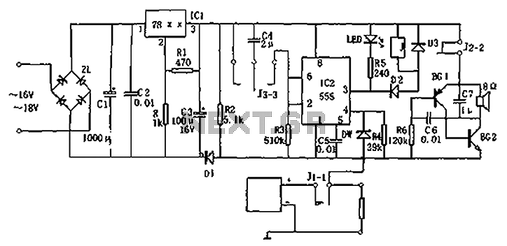
A read-only phase sequence indicator circuit

The described circuit operates based on a three-phase voltage system, where the phase relationships are crucial for determining the output states and LED indicators. The circuit utilizes diodes VD2 and VD3 for controlling the flow of current based on the phase voltage conditions. When the U terminal voltage transitions from a positive to negative state, it triggers a sequence of events that involve the IC's clock input, which is sensitive to rising edges. This ensures that the IC can effectively manage the output states based on the phase voltages.
The IC's D state is influenced by the voltage conditions at the terminal points, which are determined by the phase relationships. The design incorporates feedback from the output conditions to maintain stability and ensure proper operation of the LEDs. The green LED activation indicates a specific state of the circuit, while the yellow output signifies the synthesis of signals from the diodes.
Power management is achieved through the use of a buck rectifier, which reduces the voltage level while maintaining current efficiency. The capacitors C and C2 serve as filters to smooth out any ripples in the voltage, providing a stable power supply to the circuit. The regulator (VD7) ensures that the output voltage remains within the desired range, facilitating reliable operation of the entire system.
This circuit exemplifies the integration of phase control, signal processing, and power management, showcasing the complexities involved in designing a robust electronic system that responds dynamically to varying input conditions.As can be seen from the three-phase voltage waveform diagram [Figure 2- 76 (a)] When one of the phases voltage from positive to negative over the zero point, followed by a phas e voltage is positive, while the third group was negative. U side or t terminal voltage is positive when steady pressure diode VD2 and VD3 will produce voltage, while H and V2 will be turned on. When the U terminal voltage from positive to negative zero crossing, VD2. Voltage E reduced ov, H off, the clock pulse input of IC to get a pulse signal rising edge, the D end state is set IC.
And this time, since trade t terminal voltage, the voltage VD3 on to ov, V2 off, 0 output terminal and the D terminal of the IC as a high potential, and the hundred-ended output is low, H turned on, the lights VD green LED, shown in yellow color VD4 after synthesis. Conversely, if the U, V, IV in FIG phase relationship with the opposite one, the mine when the terminal voltage from positive to negative zero crossing, W terminal voltage will be positive, the outlet end of the IC is low, the output terminal of high insect potential, low potential output terminal 0, V4 conduction, lit VD6 green LED, VDfi shows yellow after synthesis.
Power to the entire circuit is powered by V-phase through C, and VD, buck rectifier, C2 and by the post-filter and regulator VD7 obtained.
Related Circuits
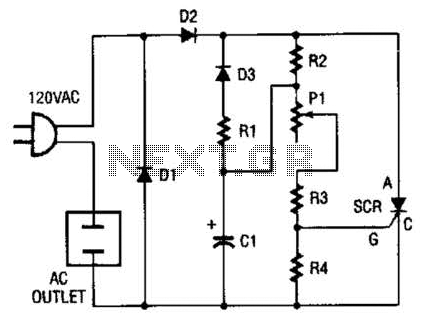
This circuit allows any standard household bulb to shimmer or blink. It is compatible with incandescent lights up to 200 W and operates on standard 120 Vac. The circuit employs a silicon-controlled rectifier (SCR) to create the shimmering effect....
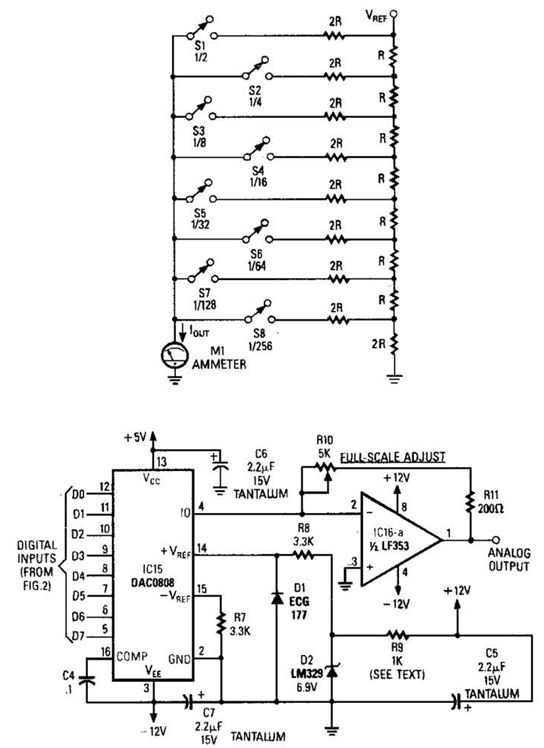
Figure A illustrates an R/2R resistor ladder. Each closed switch increases the current output. A basic channel A/D converter is depicted in Figure B. The voltage reference (D2) is shared among all channels, while the value of the dropping...
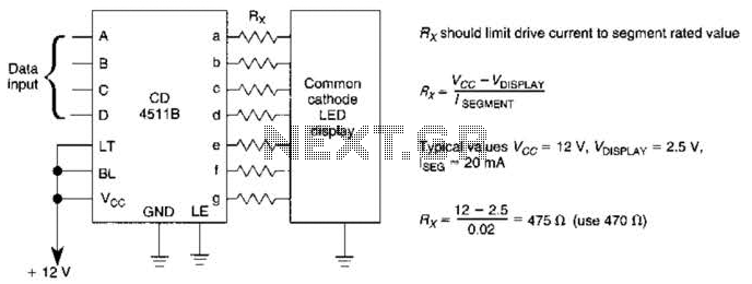
A CD4511B CMOS LED display driver can be utilized to operate a common cathode LED display. Current limiting resistors are employed to restrict the segment current to the specified value at the maximum supply voltage. The CD4511B is a...
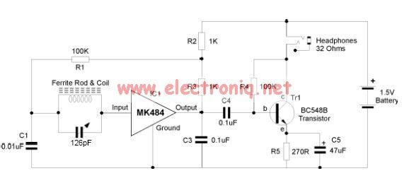
The MK484 AM radio circuit offers a comprehensive solution that includes an RF amplifier, detection, and automatic gain control (AGC) circuit. It requires only a few external components to achieve a high-quality AM tuner. The circuit features an input...
Circuit diagram for a DC power supply protection circuit. The device includes a buck rectifier power supply, a monostable delay circuit, a relay control circuit, and an audio feedback oscillation circuit. The entire circuit operates with a DC voltage...
The circuit described below monitors the car's brake lights and indicates their operational status using a 12V light-emitting diode (LED). This functionality can prevent fines for driving with defective brake lights and enhance road safety. The monitor relies on...