
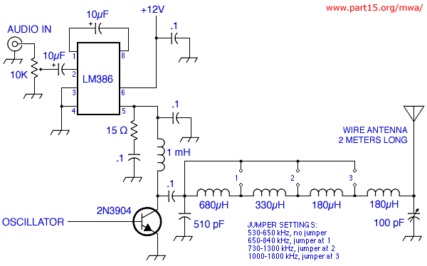
Digital To Analog Converter Circuit
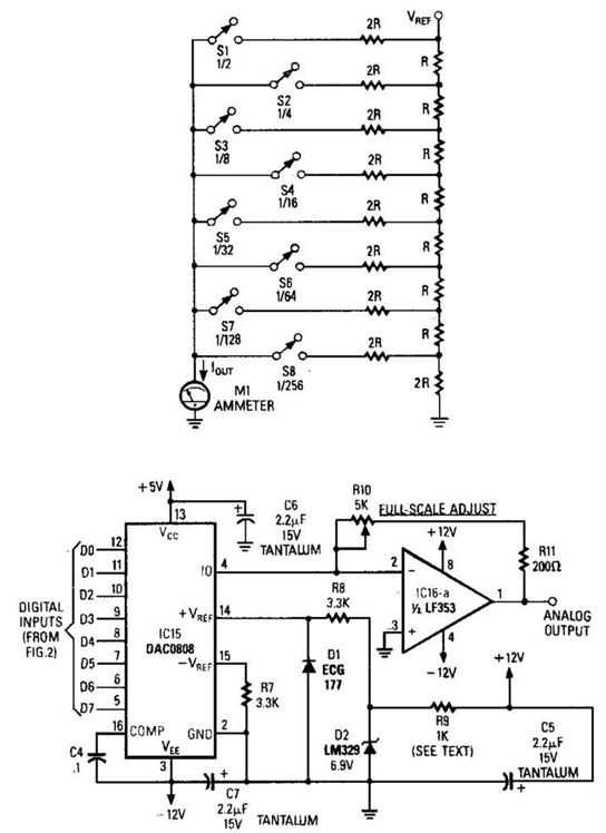
The R/2R resistor ladder is a digital-to-analog converter (DAC) configuration that utilizes a series of resistors arranged in a specific manner to create a voltage output that is proportional to the digital input. The ladder consists of resistors of two values, R and 2R, which are used to create a binary weighted output voltage. When switches corresponding to the digital inputs are closed, they effectively connect the respective resistor to the output node, thereby contributing to the total current and resulting voltage.
In the context of the A/D converter shown in Figure B, the voltage reference (D2) plays a critical role in ensuring that the analog output from the DAC is stable and accurate across all channels. The dropping resistor (R9) is essential for controlling the current flowing through the circuit, and its value must be adjusted based on the number of DACs in the system to maintain proper functionality and prevent overload.
The DAC0808, represented as IC15 in the schematic, is an integrated circuit that converts digital signals into analog voltages. It is widely used in applications where precise voltage levels are required, such as in audio and video equipment, instrumentation, and control systems. The DAC0808 features an 8-bit resolution, allowing for 256 discrete levels of output, which enhances the ability to transmit more detailed information.
In summary, the combination of the R/2R resistor ladder and the DAC0808 chip provides a robust solution for converting digital signals to analog voltages, facilitating a wide range of applications in electronic systems. Proper design considerations, including the selection of resistor values and the configuration of the voltage reference, are crucial for achieving optimal performance in such circuits.Figure A is an R/2R resistor ladder. Each switch that is closed increases the amount of current at. A simple channel A/D converter is shown in Fig. B. The voltage reference (D2) is common to all channels, but-the value of the dropping resistor (R9) varies as the number of DACs installed in the system. IC15 is a DAC0808 A/D converter chip. We aim to transmit more information by carrying articles. Please send us an E-mail to wanghuali@hqew. net within 15 days if we are involved in the problems of article content, copyright or other problems. We will delete it soon. 🔗 External reference
Related Circuits
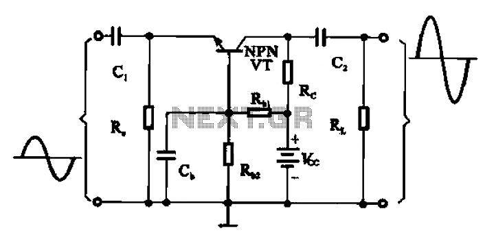
A common base transistor amplifier circuit is characterized by its basic structure, which includes key components such as a biasing resistor, capacitors for coupling, and an amplifying transistor. The circuit features four resistors that establish the quiescent point, with...
Today, it is no longer necessary to use discrete components for constructing oscillators. Many manufacturers now offer ready-made voltage-controlled oscillator (VCO) integrated circuits (ICs) that require only a few external components to determine the frequency. An example of such...
Amplifier with IC number TDA7293 for processing sound systems. This amplifier includes inputs for a radio, TV, stereo, or other line-level devices. It also features a phono input for a record player, guitar, microphone, or other unamplified sources. With...
If a complete circuit is needed, there are thousands of these circuits available in the designs. Some of them can be provided easily, but further communication is required. The request indicates a need for a comprehensive circuit design, which may...
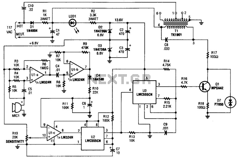
The baby-alert transmitter is constructed using an LM324 quad operational amplifier (U1), two LMC555CM CMOS oscillator/timers (U2 and U3), along with several supporting components. The transmitter activates upon detecting sound at MIC1, emitting a signal. Its operational frequency is...
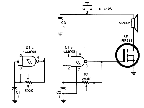
Gates U1-a and U1-b of the 4093 quad 2-input NAND Schmitt trigger are connected in variable, low-frequency square-wave oscillator circuits. The output of gate U1-a is connected to one of the inputs of gate U1-b. The square-wave output of...