
555 ultra-low frequency signal generator circuit diagram of a millivolt
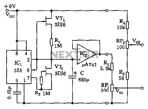
The circuit functions as a versatile signal generator, primarily designed for applications in self-balancing recorders. The inclusion of an astable multivibrator, realized through the 555 timer IC, allows for the generation of a square wave signal. This signal can be finely tuned to operate within a specified frequency range, making it suitable for various testing scenarios.
The output stage, implemented with an operational amplifier configured as a voltage follower, serves to buffer the output signal. This configuration ensures that the output impedance is significantly lower than that of the input, allowing for better interfacing with subsequent stages of the circuit or external devices. The voltage follower also prevents loading effects that could distort the signal integrity.
The adjustable output voltage, with a range of 0 to 50 mV, is crucial for applications that require precise control over signal levels. The ability to continuously adjust the output voltage at 25 mV for both positive and negative shifts enhances the circuit's flexibility, enabling it to accommodate various testing conditions.
Overall, the circuit's design leverages standard components to create a reliable and adaptable generator that can meet the needs of self-balancing recorders and other related applications, ensuring accurate signal generation and manipulation. Circuit shown in Figure generator consists of an oscillator, voltage follower, the amplitude of zero, zero shift circuit. Used as a self-balancing recorder running test signal source, output signal 0 ~ 50mV, 25mV output voltage is continuously adjustable positive and negative zero shift, the Duty Cycle 30 ~ 40Hz. IC1 (555) and VT1, VT2, R1, R2, C composition astable multivibrator, VT1, R1 and VT2, R2 respectively composed of charge and discharge current source.
IC2 operational amplifier as a voltage follower used primarily for impedance matching, low impedance output. The output voltage V0 V01-V02, by adjusting the RP1, RP2, can achieve zero amplitude level and migration.
Related Circuits
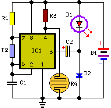
This circuit functions as a night lamp when a wall mains socket is unavailable for plugging in a continuously operating small neon lamp device. To minimize battery consumption, it utilizes a single 1.5V cell, and a simple voltage doubler...
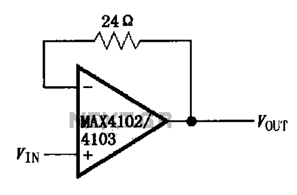
The MAX4102/4103 unity gain buffer circuit is illustrated in the figure. This circuit incorporates a small resistor (24 ohms) positioned in the feedback loop of the amplifier, which forms a unity gain buffer. Additionally, it achieves a maximum bandwidth...
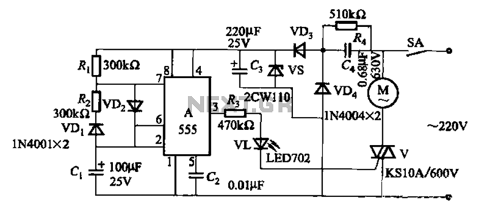
The circuit depicted in Figure 3-16 utilizes a 555 IC (Integrated Circuit) as the control element. It features a capacitive step-down circuit and incorporates a bidirectional thyristor (V) for intermittent motor control operation. By adjusting the resistance values of...
Many electronic devices rely on the shape of signals. Generating square wave signals from sine waves is relatively straightforward, while the reverse process is more challenging. The static square wave-to-sine wave converter circuit can produce an accurate sine wave...
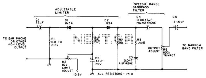
This circuit employs a diode series clipper to limit noise peaks on a received signal. It is most effective in scenarios where several volts peak-to-peak of audio signal are present. The diode series clipper circuit is designed to protect subsequent...

Useful for narrowband frequency modulation (NBFM) reception on older shortwave receivers that lack this capability, this circuit employs a phase-locked loop (PLL) integrated circuit, specifically the N565N. It was originally designed for use with an old Hammarlund HQ-170 receiver,...