
Accurate Sine Wave Generator Circuit PCB
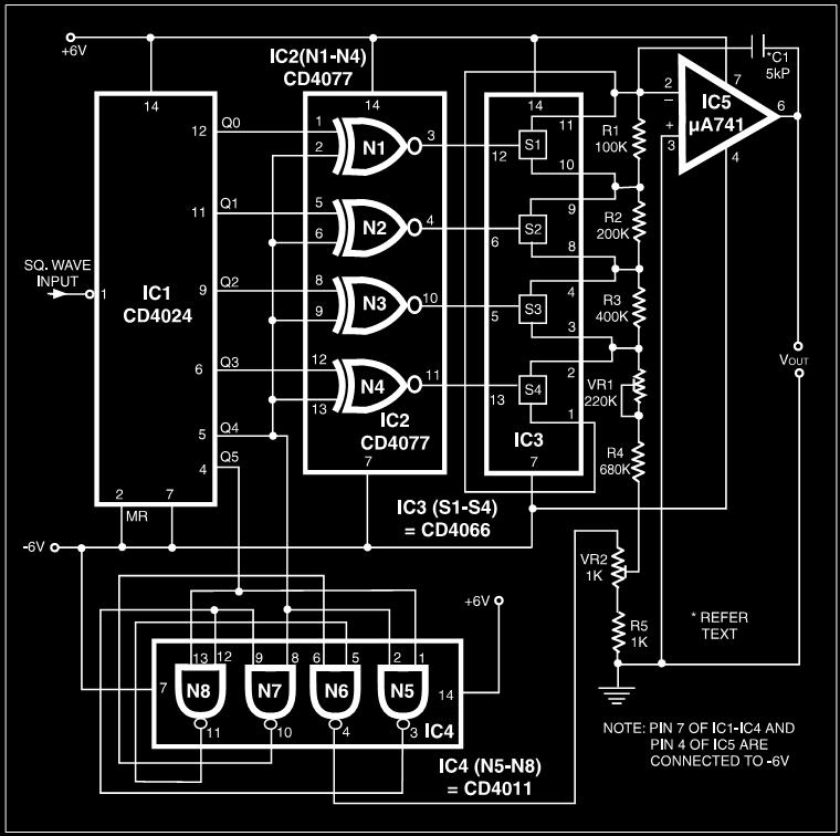
The square wave-to-sine wave converter circuit is designed to achieve high fidelity in signal shape conversion, catering to various applications in electronics where accurate waveform representation is critical. The use of the CD4024 as a counter allows for precise timing and control of the square wave input, while the integration of the CD4077B for signal processing enhances the versatility of the circuit by allowing for dual mode operation.
The CD4066 quad bilateral switch plays a crucial role in modulating the output signal, enabling dynamic control over the resistance in the feedback loop. This adaptability is essential for maintaining the integrity of the sine wave across different frequency ranges. The LM741 operational amplifier is utilized for its reliable performance in analog signal processing, facilitating the integration of the variable current through capacitor C1, which is pivotal in shaping the output waveform.
Furthermore, the circuit's reliance on CMOS technology for the majority of its components ensures minimal power consumption, making it suitable for battery-operated devices and applications where energy efficiency is paramount. The design also incorporates adjustable components, such as VR1 and VR2, allowing for real-time calibration of the sine wave output. This feature is particularly beneficial in scenarios where precise waveform characteristics are required, such as in audio applications or signal testing environments.
Overall, this square wave-to-sine wave converter circuit exemplifies a sophisticated approach to waveform generation, combining various ICs to achieve a reliable and efficient solution for electronic signal processing challenges.Many electronic devices depend upon the shape of the signals. It is very simple to produce square wave signals from sine signal, but doing vice versa is quite difficult. In case of static square wave-to-sine wave converter circuit diagram, in low frequency range, we can generate accurate sine wave, but in high frequency range the shape will not be
a true sine wave. Here is a solution to that problem as the wave does not tend to have distortion. The circuit shown here uses five ICs. The squarewave signal is fed at pin 1 of IC1 (CD 4024). IC1 is a 7-bit counter, but here only 6 bits are made use of. The first four bits are fed as a signal bus to IC3 (CD4066) quad bilateral switch through IC2 (CD4077B) that contains four exclusive NOR gates. It converts the 4-bit signal bus to up mode` and down mode` hexadecimal signals, simultaneously. The converted signal bus switches on and off the ladder switches inside CD4066. As a result, the net resistance of ladder varies. This varying resistance varies the charging and discharging current of capacitor C1 in thefeedback path of IC5 (LM741).
The charging and discharging mode is controlled by IC4 (CD4011). In fact, capacitor C1 works as an integrator. The sinewave producing circuit needs 64- bit squarewave pulse for 360o sine wave. A missing pulse in this 64-bit sequence produces ramp. In this circuit, all ICs except IC5 are CMOS ICs and hence the current consumption is very low. The value of capacitor C1 may be calculated from the relationship: C1 = 0. 27/f0 µF. The value shown in the circuit is for 50Hz output frequency. The shape of the sinewave output may be corrected using presets VR1 and VR2. 🔗 External reference
Related Circuits
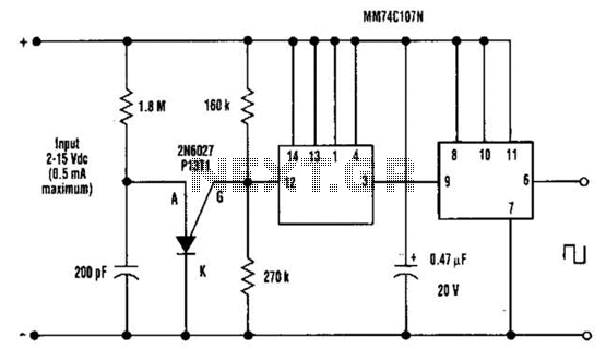
A direct current (DC) voltage source within the range of 2 to 15 volts can be converted into a unipolar square wave. This square wave has a peak amplitude that is nearly equal to the DC source voltage, with...
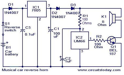
This circuit is designed to produce a musical horn whenever a car is in reverse gear. It utilizes two integrated circuits (ICs) for its operation: a voltage regulator (7805, referred to as IC1) and a musical tone generator (UM66,...
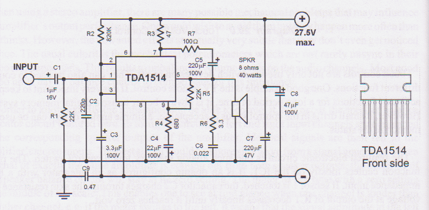
This is a compact, easy-to-build amplifier that utilizes a single integrated circuit (IC) to deliver 40 watts of audio power. It is well-suited for amplifying audio signals from devices such as mobile CD players or iPods. The integrated circuit...
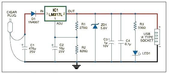
USB car charger adapter circuit design using LM317 regulator circuit The USB car charger adapter circuit utilizing the LM317 voltage regulator is designed to convert a car's 12V DC power supply into a stable 5V output, suitable for charging USB-powered...
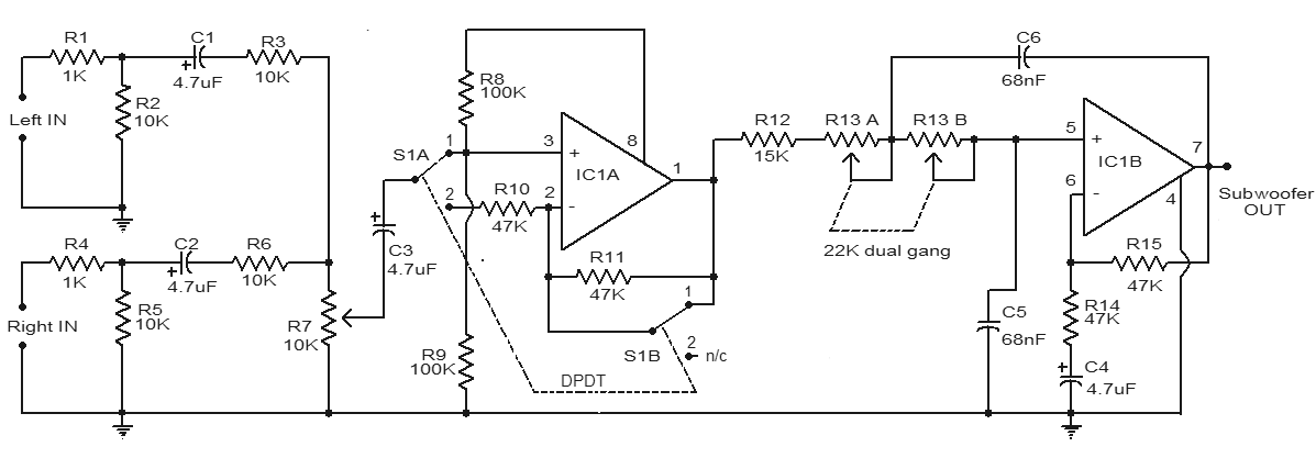
This is a simple subwoofer filter circuit that can be powered by a 12V DC source. It is particularly useful in automotive applications for subwoofers. The circuit functions as a low-pass filter, with a pass frequency adjustable between 60...
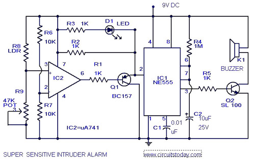
The circuit diagram illustrates an ultra-sensitive intruder alarm. The mere shadow of an intruder passing within a few meters of the circuit is sufficient to activate the alarm. In this setup, the IC2 uA741 is configured as a sensitive...