
0 1000 volt regulated high voltage
The high-voltage DC-DC converter circuit is designed to efficiently convert low-voltage AC input into a high-voltage DC output. The circuit begins with an AC input of 12V at 800mA, which is fed into a bridge rectifier composed of four diodes configured to convert the AC voltage to pulsating DC. The output from the rectifier is then smoothed using capacitors to reduce ripple, ensuring a stable DC voltage.
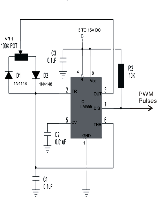
The adjustable output voltage feature is achieved through a feedback mechanism integrated with the 555 timer IC, which functions as a pulse-width modulation (PWM) controller. The PWM signal regulates the switching of the MOSFETs, allowing for fine-tuning of the output voltage within the specified range of 0-1000V DC. The CMOS IC 4001 serves as a logic gate that can be used for additional control functions within the circuit, enhancing its operational capabilities.
The 7805 voltage regulator is included to provide a stable 5V output, which can be used to power other low-voltage components within the circuit. The incorporation of NPN transistors allows for additional amplification and switching capabilities, ensuring that the circuit can handle the high voltage and current demands effectively.
The IRF510 MOSFETs are critical components in this design, acting as the final amplification stage. They are capable of handling high voltages and currents, making them suitable for applications requiring significant power output. The design allows for flexibility in component selection; if the specified transformer or other components are not available, alternatives can be utilized as long as they meet the necessary voltage and current ratings.
Overall, this high-voltage DC-DC converter circuit exemplifies a robust design that emphasizes performance and adaptability, making it suitable for various applications that require high-voltage DC power conversion.Input voltage from aerial voltage DC DC advocate is 12V AC at 800mA accepted and again adapted to DC through a arch rectifier Diode 1A. The voltage achievement of advocate ambit can be adapted in the ambit of 0-1000V DC. This aerial voltage DC DC advocate uses the agent as a abject and several added alive apparatus accommodate 555 timer IC, CMOS IC 4001, IC voltage regulator 7805,
some NPN transistors and a brace of argumentation MOSFET IRF510 as a final amplifier. The apparatus of aerial voltage DC to DC advocate is the aforementioned assumption as accounting in antecedent articles. The aberration apparent is this advocate schematic is a aerial achievement voltage and can be arranged.
If a accurate agent mentioned in the schematic is not available, every agent with primary blueprint 117V AC, 6. 3V AC CT accessory to work. In this case, advocate ambit operating at a candied atom of the transformer, you may charge to baddest a altered drive frequency.
🔗 External reference
Related Circuits
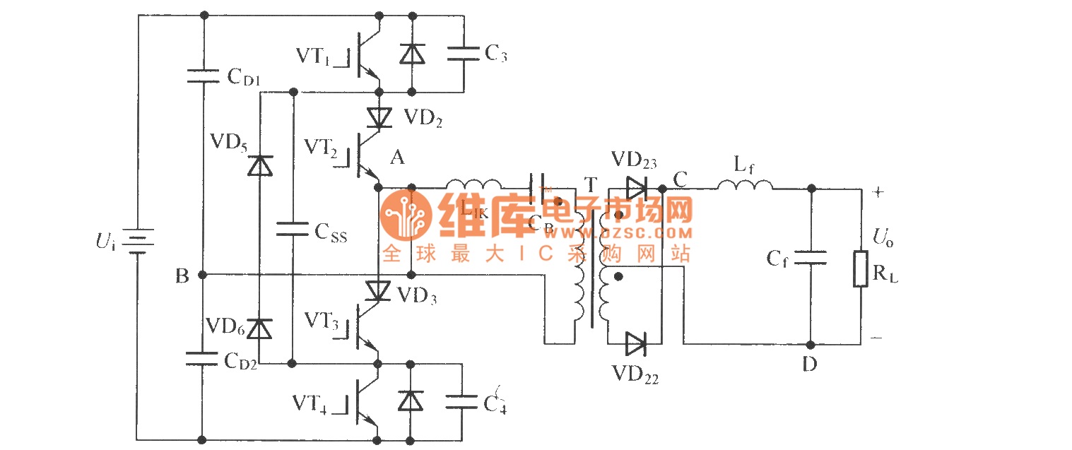
To eliminate circulating current in a zero-voltage switch three-level DC converter during its zero state, a zero-voltage zero-current switch three-level DC converter circuit has been proposed. The primary distinction between this circuit and the standard zero-voltage switch three-level DC...
The configuration presented in the diagram below is a simple MOSFET-based design intended for amplifying current at ±60 volts, allowing the connected transformer to generate a required output of 1 kVA. The components Q1 and Q2 form the initial...
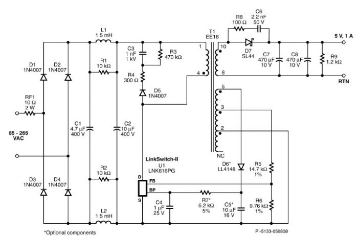
A very simple 5-volt constant voltage, constant current (CV/CC) universal-input power supply for cell phone or similar charger applications can be designed using the LNK616PG product from the LinkSwitch-II family. This low-cost charger adapter accepts a wide range of...
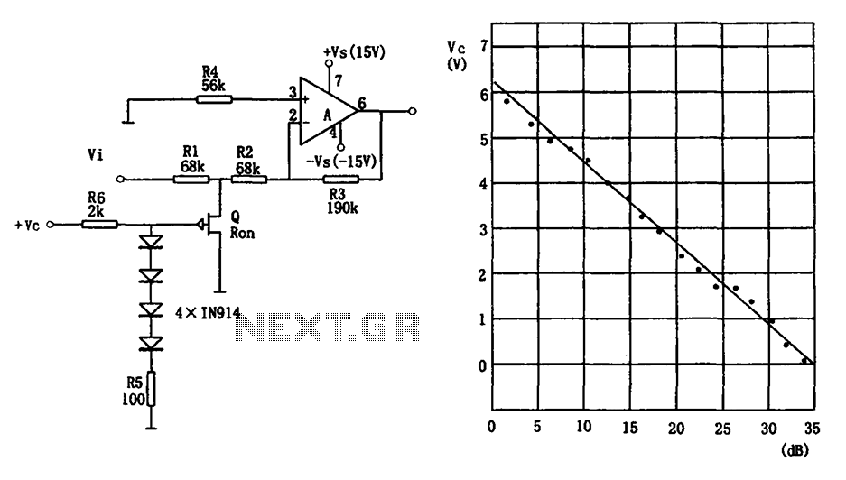
The voltage-controlled gain amplifier utilizes a FET gate voltage and the drain-source resistance (RSD) to approximate a logarithmic relationship. The integrated circuit chip LM307 is employed in the amplifier circuit with the inverting input configuration. In the circuit, RSD...
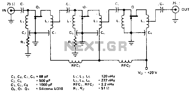
The amplifier circuit is designed for a center frequency of 225 MHz, with a bandwidth of 50 MHz at 1 dB, low input voltage standing wave ratio (VSWR) in a 75-ohm system, and a gain of 24 dB. Three...

The preamp being discussed features optional tone and balance controls. While these can be omitted if desired, it is generally not recommended. The input switching capability of this preamp can be extended to accommodate additional signal sources if required. However,...