
LNK616PG 5 volt constant charger circuit design electronic project

The power supply circuit described employs the LNK616PG from the LinkSwitch-II series, which is specifically designed for applications requiring a compact and efficient power solution. The device operates within a wide input voltage range, making it suitable for global use. The internal switching MOSFET allows for efficient energy conversion, while the ON/OFF control helps in reducing power consumption when the load is not present.
The rectification process is accomplished using a bridge rectifier configuration with diodes D1 through D4, converting the AC input to a pulsating DC voltage. The bulk storage capacitors C1 and C2 smooth out the pulsating DC, providing a stable voltage level for further processing. The use of pi filters created by inductors L1 and L2 in conjunction with capacitors C1 and C2 is essential for minimizing electromagnetic interference (EMI) that could affect other devices in proximity. This filtering ensures compliance with EMI regulations while maintaining signal integrity.
The transformer T1 plays a crucial role in isolating the output from the input, providing both voltage transformation and safety isolation. The control circuitry, which includes the internal MOSFET of U1, regulates the output voltage and current to ensure that the specified 5V at 1A is consistently delivered to the load.
To protect the circuit from voltage spikes that may occur due to leakage inductance, an RCD-R clamp is implemented. This clamp comprises diodes D5, resistors R3 and R4, and capacitor C3, effectively shunting excess energy away from the MOSFET and preventing damage from high-voltage transients.
Overall, this design illustrates a robust and efficient solution for powering devices such as cell phones, ensuring reliability and adherence to electrical standards.A very simple 5 volt constant voltage, constant current (CV/CC) universal-input power supply for cell phone or similar charger applications can be designed using the LNK616PG product from the LinkSwitch-II family. As you can see in the circuit diagram, this low cost charger, adapter accepts a wide range of input voltage, from 85 VAC up to 265 VA
C and will provide a fixed 5 volt DC output at a maximum output current of 1 ampere. The LNK616PG has an integrated 700 V switching MOSFET and ON/OFF control function which together deliver high efficiency under all load conditions and low no-load energy consumption. The AC input power is rectified by diodes D1 through D4. The rectified DC is filtered by the bulk storage capacitors C1 and C2. Inductors L1 and L2, with capacitors C1 and C2, form pi filters to attenuate conducted differential-mode EMI noise.
The rectified and filtered input voltage is applied to one end of the transformer (T1) primary winding. The other side of the transformer`s primary winding is driven by the internal MOSFET of U1. An RCD-R clamp consisting of D5, R3, R4, and C3 limits drain voltage spikes caused by leakage inductance.
🔗 External reference
Related Circuits
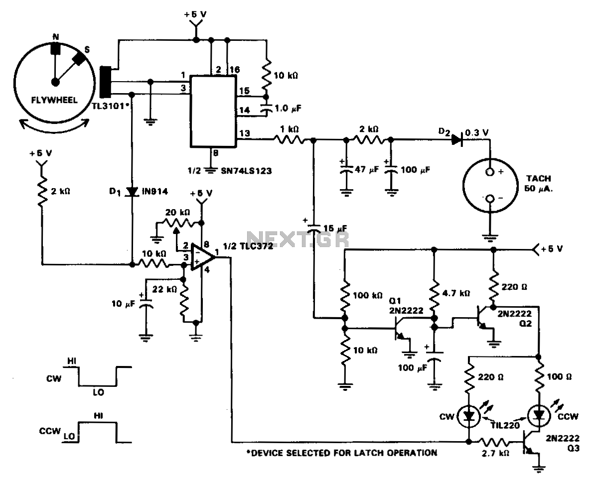
In machine and equipment design, certain applications necessitate the measurement of both shaft speed and direction of rotation. The circuit of a tachometer, which also indicates the direction of rotation, is illustrated. A flywheel is equipped with two magnets...
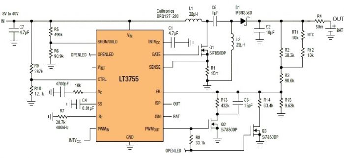
This Sealed Lead Acid Battery Charger is designed using the LT3755 DC-DC controller. The LT3755 is a DC-DC controller that operates as a constant-current source and supports a wide input voltage range from 4.5 to 40 volts, providing a...
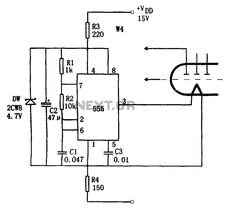
The economic fluorescent display circuit is illustrated in the figure. The primary component of this circuit is the 555 timer configured as a multivibrator. The oscillation frequency is determined by the components R1, R2, and C1, with a frequency...
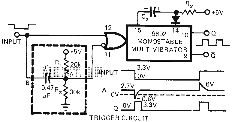
The 9602 multivibrator circuit can trigger either the rising edge or the falling edge of a square wave, but not both simultaneously. To enable double-edge triggering, two additional resistors and a capacitor can be employed. When the input signal...
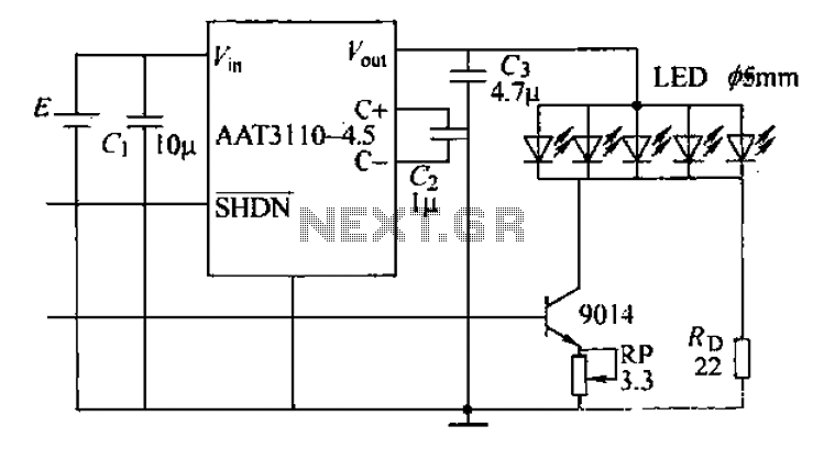
A circuit designed for a phone photo camera flash that delivers a peak current of 200mA. It utilizes the AAT3110-4.5 capacitive charge pump chip to boost and regulate the lithium battery voltage to 4.5V. This voltage powers a series...
This circuit features automatic exit and entry delays, a timed bell cut-off, and a system reset. It accommodates both normally-open and normally-closed switches, making it compatible with various input devices such as pressure mats, magnetic reed contacts, foil tape,...