
Voltage controlled gain amplifier LM307
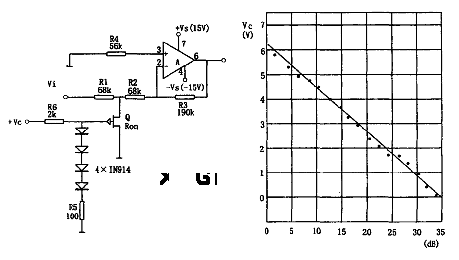
The voltage-controlled gain amplifier circuit employs a Field Effect Transistor (FET) to modulate gain based on an input control voltage. The configuration utilizes the LM307 integrated circuit, which is designed for operational amplifier applications, particularly in analog signal processing. The circuit's inverting input is critical for establishing the desired gain characteristics.
The resistors R1 and RSD form a voltage divider that determines the input voltage (Vi) to the amplifier. The diode (1N914) introduces a specific forward voltage drop that affects the gate voltage (VG) of the FET, which is essential for controlling the amplifier's gain. The relationship between the control voltage (VC) and the gain is nonlinear; as VC increases, the gain of the amplifier increases due to reduced attenuation. This behavior allows for precise control over the output signal, making it suitable for applications requiring variable gain.
The gain equations provided (Avmax and Avmin) outline the maximum and minimum gain states of the amplifier, depending on the control voltage. The maximum gain occurs when the control voltage is at its highest (7V), while the minimum gain is observed when the control voltage is at its lowest (0V). The circuit's performance is heavily influenced by the selected resistor values (R1, R2, R3, and RSD), which dictate the gain levels.
The upper cutoff frequency of the amplifier is determined by the low-pass filter characteristics, which consist of the resistor R1 and the capacitance associated with the FET. This cutoff frequency is a critical parameter for applications where bandwidth is a consideration. The stated maximum cutoff frequency of 1.8 MHz indicates the frequency range over which the amplifier can effectively operate without significant attenuation of the signal.
In summary, this voltage-controlled gain amplifier circuit exemplifies the integration of analog components to achieve variable gain control, suitable for a variety of signal processing applications. The LM307 integrated circuit serves as a robust platform for implementing these functionalities, with careful attention to the selection of passive components to optimize performance. As shown for the voltage-controlled gain amplifier. Use FET gate voltage and the drain - source resistance between RSD to approximate logarithmic relationship may constitute a voltage-controlled gain amplifier. The integrated circuit chip LM307 amplifier circuit, take the inverting input. Figure (a) shows that, RSD and R1 form a voltage divider (for Vi partial pressure). 4 1N914 diode voltage drop and the voltage drop across the resistor R5 and the gate voltage VG is equal to the FET. The VG control voltage VC is nonlinear, but the amount of attenuation control voltage VC and the amplifier gain corresponding relationship as shown in (b) below.
Figure (b) shows that the larger the control voltage VC, the smaller the amount of attenuation of the amplifier gain, that is, when VC 7V, amplifier gain maximum (minimum attenuation); when VC 0V, the maximum amount of attenuation of the amplifier gain ( the minimum gain). Figure (a) shows the maximum and minimum gain of the circuit is: When VC 7v, the maximum gain is: Avmax -R3/(R1 + R2).
When VC 0V, the minimum gain is: Avmin -R3/(R2 // RSD + R1). The circuits upper cutoff frequency depends on the low-pass filter between R1 and FET capacitance posed. For the FIG. (A) component parameters as shown in its worst upper cut-off frequency up to 1.8MHz, the value in the case of VC 7V measured (ie, the maximum gain of the circuit is measured).
The main parameters (typ) LM307 integrated chip
Related Circuits
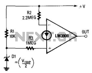
The output becomes high when the supply voltage drops below a threshold set by the zener diode D1. If D1 is a 5.6-V zener diode, the operational amplifier will activate when the supply voltage decreases to around 11 V....
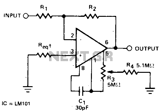
The required resistance (Req) may be zero or equal to the parallel combination of resistors R1 and R2 to achieve minimum offset. The circuit configuration described involves the use of two resistors, R1 and R2, connected in parallel. In a...
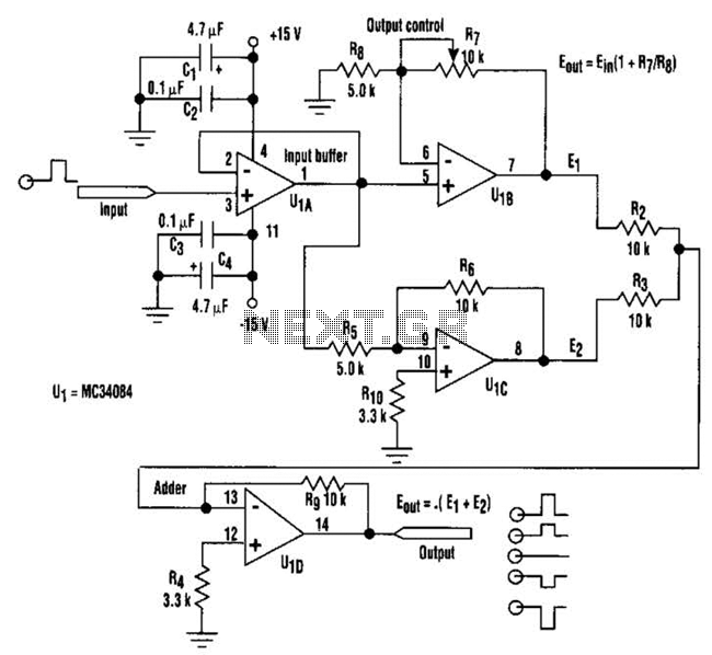
By adjusting one potentiometer, the output of this circuit can be varied from a positive version of the input signal, smoothly transitioning through zero output, and then to a negative version of the input. For instance, if the input...
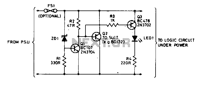
The Zener diode ZD1 monitors the supply voltage, and if the supply exceeds 6 V, transistor Q1 will activate. This activation causes transistor Q2 to conduct, thereby clamping the voltage rail. The subsequent behavior of the circuit is contingent...
A MOSFET solid-state kilowatt amplifier using MOSFETs. Helge's work was followed by articles that appeared in QEX and QST by Joel F. Paladino, N6AMG. Since then, very little has been written in amateur radio publications concerning MOSFETs in kilowatt...
The microphone has high sensitivity in the audio range, but in the ultrasonic range, the sensitivity decreases rapidly. The receiver is very sensitive. To prevent overdriving and feedback due to the high sensitivity of the microphone in the audio...