
0-30 Volt Laboratory Power Supply
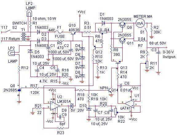
The circuit described features a power-on indicator lamp (LP2) that illuminates when the device is powered. This serves as a visual confirmation of the operational status of the device. An additional lamp is activated when the unit reaches a specified current limit, providing an alert to the user that the current threshold has been met, which is critical for applications requiring current monitoring.
The capacitor multiplier configuration involving resistor R5, capacitor C2, and transistor Q10, which is housed in a TO-3 package, enhances the effective capacitance seen by the circuit. This arrangement allows for better voltage regulation and reduced ripple in the power supply, which is particularly important in precision analog applications.
A 36-volt zener diode placed across capacitor C2 serves as a voltage limiter for the supply voltage to the operational amplifiers (op-amps). This component ensures that the voltage supplied to the op-amps does not exceed a safe operating level, thereby protecting them from potential damage due to overvoltage conditions.
The circuit also incorporates diodes D5, capacitors C4 and C5, and resistors R15 and R16, which together create a small negative voltage supply. This negative supply is essential for the proper operation of the op-amps, allowing them to function down to zero volts at their output pins (pin 6). This capability is particularly useful in applications requiring signal processing that may involve negative voltage levels.
In modern circuit design, it is noted that the components providing the negative supply could potentially be replaced with a more streamlined approach using CMOS rail-to-rail op-amps. These op-amps can operate effectively across the full range of supply voltages, eliminating the need for additional components to generate a negative supply, thereby simplifying the design and improving reliability. This transition to more advanced components reflects ongoing trends in electronics towards greater efficiency and miniaturization.With reference to the schematic, lamp, LP2, is a power-on indicator. The other lamp (lower) lights when the unit reaches its preset current limit. R5, C2, and Q10 (TO-3 case) operate as a capacitor multiplier. The 36 volt zener across C2 limits the maximum supply voltage to the op-amps supply pins. D5, C4, C5, R15, and R16 provide a small amount of negative supply for the op-amps so that the op-amps can operate down to zero volts at the output pins (pins 6). A more modern design might eliminate these 4 components and use a CMOS rail-to-rail op-amp. 🔗 External reference
Related Circuits

This is an inexpensive DC voltage doubler circuit diagram that requires a minimal number of components and is capable of delivering 10V from a 5V power supply. If the oscillator needs to be... The circuit operates on the principle of...
This simple circuit tests speakers, microphones, transformers, and voltage. It is essentially a very low-frequency oscillator that produces extremely short pulses. The sound produced is easy to hear and helps determine the precise direction it originates from, making it...
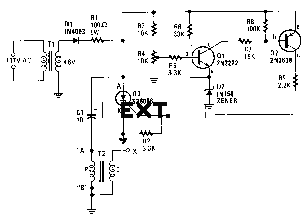
A step-down transformer T1 reduces the incoming line voltage to approximately 48 Vac, which is then rectified by diode D1. The resulting direct current charges capacitor C1 through a current-limiting resistor R1 to a voltage level set by R4....
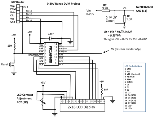
This project details the construction of a digital voltmeter utilizing a PIC microcontroller. A character-based HD44780 LCD display is employed to visualize voltage measurements. The microcontroller selected for this project is the PIC16F688, which features 12 I/O pins, with...
The circuit illustrated relates to a standard industrial UPS (Uninterruptible Power Supply), demonstrating how the batteries assume control during an electrical outage. The Uninterruptible Power Supply (UPS) circuit typically consists of several key components that ensure a reliable power supply...

This 15V variable power supply electronic project is designed using 2N3055 transistors. The output voltage of this variable power supply can be adjusted in the range between 1.5 and 15 volts. This 2N3055 15V variable power supply can provide...