
0-50V 1A power supply with CA3086
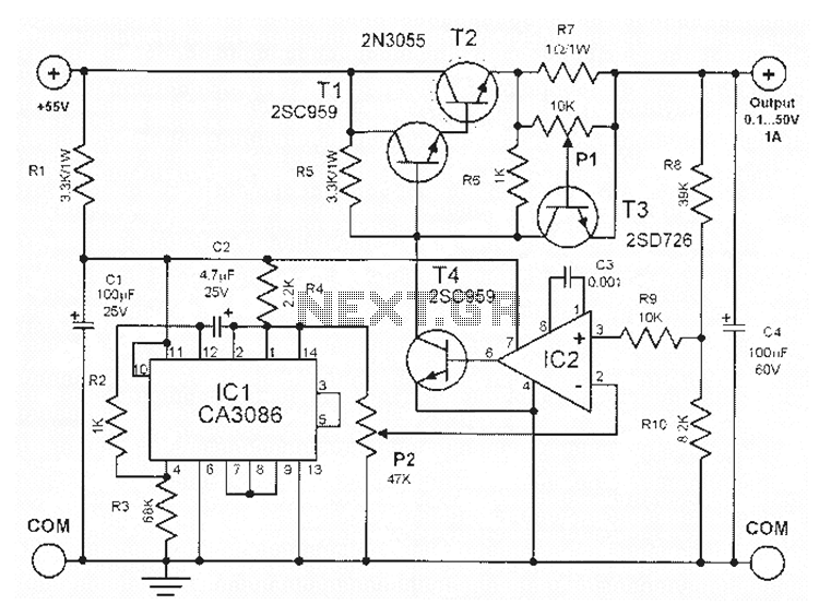
This power supply circuit is designed to maintain a highly stable output voltage across a wide range of load conditions and input voltage fluctuations. The circuit features an operational amplifier (opamp) CA3130, which plays a critical role in voltage regulation. The opamp compares the reference voltage, generated by a temperature-compensated transistor array (IC1), to the output voltage. This arrangement ensures minimal voltage drop (0.005%) under varying load conditions from 0% to 100%.
The reference voltage is established through a potentiometer (P1), allowing for fine-tuning of the output voltage, which can be adjusted from 0.1V to 50V. The temperature-compensated array consists of five transistors, with four functioning as reference diodes and the fifth controlling the output impedance, providing stable performance over temperature variations.
The opamp's output is connected to a voltage divider, which scales down the output voltage before it is fed into the non-inverting input of the opamp. This feedback mechanism is essential for achieving precise voltage regulation. The circuit incorporates a Darlington pair configuration using transistors T1 and T2, which enhances current amplification, ensuring that the output can handle significant loads.
Transistor T3 serves as a current limiter, providing protection against overcurrent conditions. The current limit is adjustable via the potentiometer P1, with a minimum threshold of 0.6 amperes. When P1 is set to its maximum position, the current limiting feature is effectively disabled, allowing for maximum current delivery to the load.
Transistor T4 is employed to elevate the output voltage while isolating the opamp from the higher voltage levels present at the output. This isolation is crucial for protecting the sensitive components of the circuit while maintaining operational integrity.
Overall, this power supply circuit exemplifies advanced design principles in voltage regulation and current limiting, making it suitable for applications requiring high stability and adaptability in output voltage across varying conditions.This power supply circuit is highly stabilized that its output voltage will drop only 0.005% even though the load changes from 0 to 100%. Another excellent capability is that the output voltage will change only by 0.01% if the input voltage fluctuates.
The capability if the circuit to be adjusted from 0.1V up to 50V is due to the application of opamp IC CA3130 in the circuit. Transistor T4 raises the output voltage to higher level, and at the same time it separates the lower level opamp from the high level of the output voltage.
The reference voltage is supplied by IC1. It is a temperature compensated transistor array with 5 transistors. Four of these transistors are used as reference diodes and the fifth one sets the output impedance of the reference source. The reference voltage is set through P1. The opamp CA3130 compares the reference voltage at its minus input to the output voltage at its input.
The output voltage passes first through a voltage divider before it is fed into the plus input of the opamp. Transistors T1 and T2 work as darlington pair and amplifies the current. Transistor T3 functions as current limiter. The current limit is ajustable through P1, and the lowest current limit is 0.6 ampere. Once potentiometer P1 is set at maximum, current limiting is disabled. 🔗 External reference
Related Circuits
In a power supply circuit with a rating of 15V and a 10W power load, there are notable differences between two circuit configurations. The first configuration (A) uses discrete components in place of an integrated operational amplifier for the...
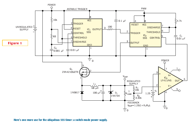
Most switch-mode power supplies utilize a PWM (pulse-width-modulated) output that is regulated through voltage feedback. A 555-timer IC can be used to generate PWM at a low cost. The circuit diagram illustrates how to convert a 555 PWM circuit...
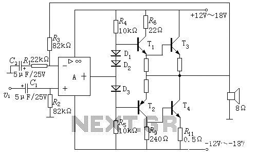
The amplifier drives a pair of loudspeakers using two LM3876 integrated power amp ICs (50 watts per channel), or a pair of headphones via a Meier crossfeed filter and an OPA2134 dual opamp. It provides four switchable line level...
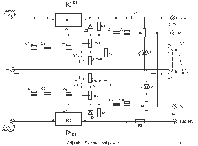
This is the voltage converter to get the voltage of ±1.25-30V from the input voltage of ±35V. I am using the 3 terminal voltage regulator for the voltage to be changed in this unit. As the regulator, LM317 is...
The first time a user signs into developerWorks, a profile is created. Certain information in the profile, including name, country or region, and company, is publicly displayed and will accompany any content posted. Users have the option to update...
The presented design features an unconventional arrangement that provides certain advantages compared to traditional designs. To begin with, a linear power supply incorporates a transformer that steps down the line voltage to a level higher than the regulated output...