
555 Timer As A Switch-Mode Power Supply

The circuit employs two 555 timer ICs to generate a PWM signal that is essential for the operation of the switch-mode power supply. The first 555 timer (IC1) operates in astable mode, generating a continuous square wave at a frequency of approximately 60 kHz. This frequency is chosen to optimize the switching performance and efficiency of the power supply. The duty cycle is adjusted so that the output remains low for about 2.5 µsec, which serves as the trigger for the second 555 timer (IC2), configured in PWM mode. The PWM output of IC2 is critical for regulating the output voltage of the power supply.
The feedback mechanism is established through the use of a voltage divider formed by resistors R1 and R2, with V1 providing a reference voltage. The output voltage can be calculated using the formula VOUT = V1(R1/R2 + 1), which allows for precise control over the output voltage based on the resistor values. The TL431 voltage reference is a reliable choice for providing the necessary 1.25V reference voltage.
The design also incorporates a zener diode (D1) for voltage spike protection, ensuring the stability of the circuit during transient conditions. The choice of components, including the selection of Q1 with low RDS(ON) characteristics, contributes to the overall efficiency and reliability of the circuit.
In terms of power handling, the circuit is capable of delivering 5V at a current of 1.5A, with an input voltage range that allows for versatility in various applications. The efficiency ratings at different input voltages indicate the performance characteristics of the design, with considerations for efficiency losses at lower load conditions. Overall, this switch-mode power supply design demonstrates a compact and efficient approach to voltage regulation using widely available components.Most switch-mode power supplies rely on a PWM (pulse-width-modulated) output that is controlled via voltage feedback. A 555-timer IC can inexpensively perform PWM. The circuit in Figure 1 shows how to turn a 555 PWM circuit into an switch-mode power supply with only one simple equation.
The design uses two 555s. IC1, in astable mode, triggers IC2in PWM mode. IC1 is set to oscillate at approximately 60 kHz at a high duty cycle. The output is low for only approximately 2. 5 µsec to trigger the PWM circuit and then goes high for the rest of the period. The PWM circuit has a maximum pulse width of approximately 85 µsec, and it becomes shorter, depending on the control voltage from the feedback circuit. You can reduce the chip count by using a 556 or another continuous-trigger source. The input must be (1. 5VOUT+Margin), so for 5V output you need 9V minimum input. If you use CMOS chips and small timing capacitors C1 and C2, you can keep the operating current low. Thus, you can use a simple zener-diode regulator for the 555 and increase the input voltage to more than 30V.
The input-voltage limit is a function of how much power the zener supply can handle while delivering 5 to 10 mA to the 555s. Q1 has low RDS(ON) and low VGS and can handle more than 40V. D1 clamps any voltage spikes, such as those that occur when a large current flow ceases, causing a large magnetic field to be left in the inductor.
You should select D1 according to the output voltage you need. For 5V output, use a 5. 6V zener diode, for example. IC3, R1, R2, and V1 form the feedback circuit to set the output voltage. The output-voltage equation is VOUT=V1(R1/R2+1). The TL431 is a popular part for setting a voltage reference and can easily create the 1. 25V shown for V1. You can supply 5V at 1. 5A with an input of 9 to 40V. At voltages higher than 12V, you can add a 10V zener-diode supply for the chips. The zener supply only slightly reduces the efficiency. With 12V input, 5V, 1. 5A output efficiency is approximately 70%, and it drops to 65% with a 40V input and a zener circuit. The zener diode`s influence is more noticeable at lower current levels; at a 50-mA load the efficiency drops to approximately 50%. 🔗 External reference
Related Circuits
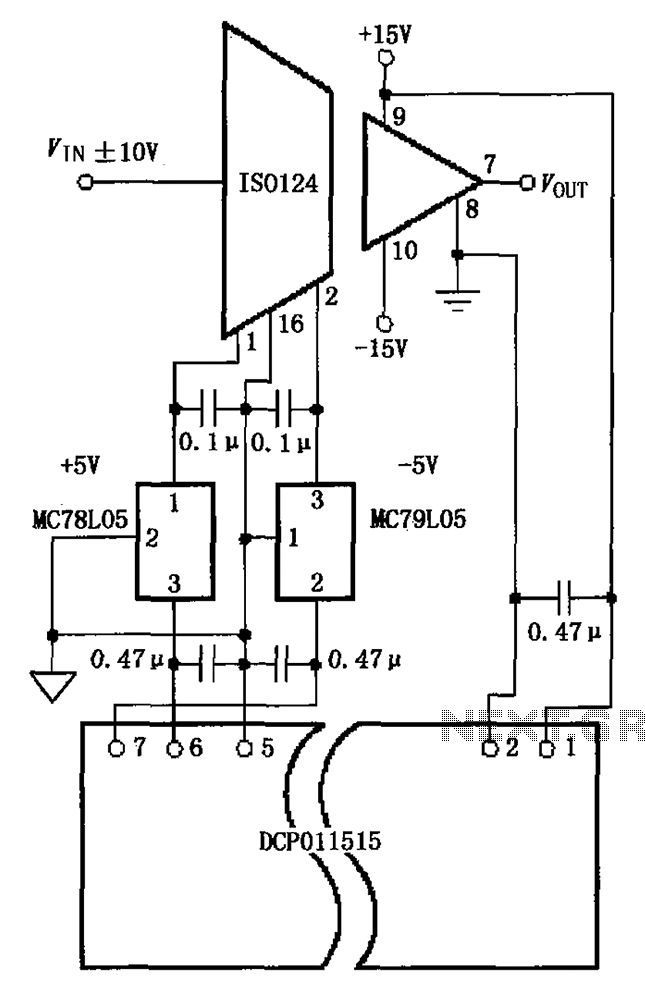
The circuit depicted in the figure includes the ISO124 and MC78L05 components, along with an external regulator, MC79L05, and the DCP011515, which collectively enhance the power supply rejection ratio (PSR) of the circuit. The input signal, VIN (maximum swing...
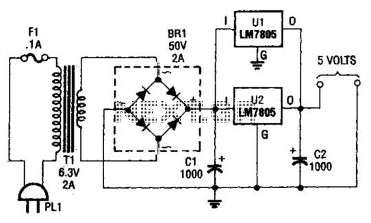
This DC supply is excellent for operating battery-powered antique radios, as it is designed to prevent damage to the tube filaments. The circuit is useful for powering the filaments of 00-A, 01-A, 112A, and 71A tubes, which require 5V...
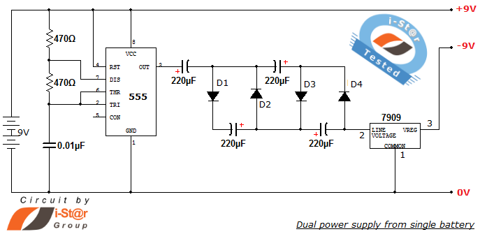
How to create a dual power supply unit using a single battery for laboratory purposes. Dual voltage power supplies are particularly needed for operational amplifier experiments and some instrumentation amplifiers. Additionally, certain low-power audio preamplifiers also require dual voltage...
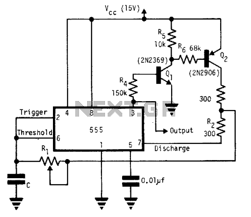
A single timing resistor ensures that the output is a square (50% duty cycle) wave at all frequency settings. Any 555 type of chip will do the job. The circuit utilizes a 555 timer IC configured in astable mode to...
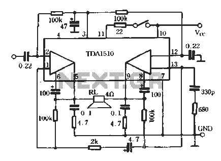
TDA1510 is an audio power amplifier from Philips. This integrated circuit (IC) includes features such as load short protection, open load detection, and an overheat protection circuit. It offers stable output voltage, excellent ripple rejection performance, requires fewer external...
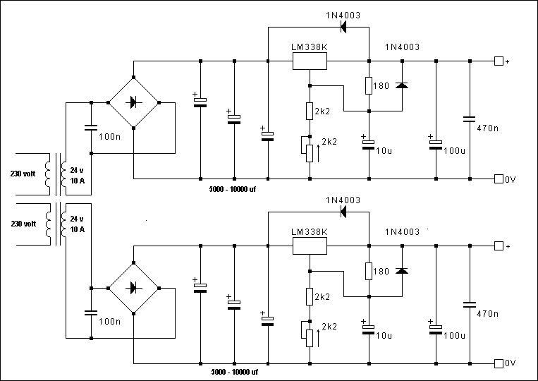
This LM338-based power supply can deliver approximately two outputs of 12 to 36 volts at 5 amps each (10 amps in version 2 of this power supply, which includes transistors to increase the current capacity). The design utilizes two...