
10 or more switches using a microcontroller
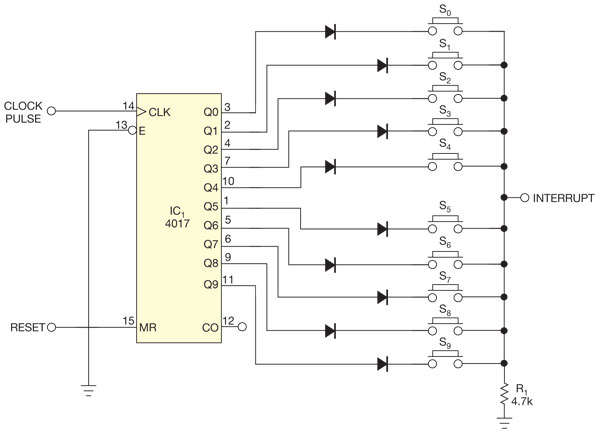
The described circuit provides an efficient method for interfacing multiple switches with a microcontroller while minimizing the number of required I/O pins. By leveraging the capabilities of the CD4017 Johnson counter, this design allows for the expansion of switch inputs beyond the initial ten, accommodating additional switches through cascading. The use of diodes ensures that simultaneous switch closures do not lead to erroneous outputs, thereby enhancing the reliability of the system.
In practical implementation, the MCU's timer interrupt plays a crucial role in maintaining the timing necessary for accurate polling of switch states while preventing potential conflicts caused by mechanical switch bounce. The design's flexibility allows for the addition of more switches without necessitating additional I/O pins, making it particularly suitable for applications where pin availability is limited.
Furthermore, the periodic hardware reset feature is essential for maintaining synchronization between the MCU and the CD4017, especially in environments susceptible to EMI and ESD interference. The ability to utilize high, low, and high impedance states on a single I/O pin for clocking and resetting the counter illustrates the ingenuity of the design, optimizing the use of available resources while ensuring reliable operation.
Overall, this circuit design exemplifies an effective approach to managing multiple switch inputs within constrained hardware environments, balancing complexity and functionality to meet the demands of various applications.There are several ways to read multiple switch inputs using a reduced number of microcontroller-unit (MCU) pins. For example, you can use an analog MCU pin to read multiple switches by assigning a unique voltage to each switch through a resistor network, or you can use a one-wire device, such as the Maxim DS2408 8-channel addressable switch.
The f irst method has several disadvantages: The MCU has to have an ADC function, debounce wait times reduce the polling rate, and an error results if the switch is opened during the ADC sampling time. The second method also has the drawback of comparatively low speed; it uses 1-wire communication, which requires continuous polling; and each poll generates an 8-bit data sequence relevant to switch positions.
This Design Idea describes a method for reading multiple pushbuttons or open/closed switches using only two digital I/O pins and a timer interrupt of the MCU (Figure 1). Optionally, a third I/O pin can be assigned to periodically reset the CD4017 (a cascadable decoded 1-of-10 Johnson counter) for reliable operation should an EMI or ESD event occur that could falsely clock the counter, or you can use the circuit shown in Figure 2 and retain the two-pin feature.
The diodes isolate the counter outputs in the event that two or more switches are closed at the same time. You can increase the number of switches connected by cascading multiple CD4017 ICs using a carry-out signal (pin 12) and a clock signal (pin 14).
Figure 1 You can easily expand this circuit to many more than 10 switches, yet still use only two MCU I/O pins, by cascading multiple CD4017 counters through their carry-outs to the following enables. Reliable operation following the initial power-up reset depends on the CD4017 counter`s remaining synchronized with the MCU counter.
This synchronization can be upset by an ESD or EMI event such as a nearby cell phone, so it would be wise to include in the firmware a periodic hardware reset to the CD4017 to keep the counts synchronized. Figure 2 shows how you can do this without having to use a third MCU pin. For this function, you use the MCU`s ability to keep its I/O pin in three different states: high, low, and, by temporarily changing the pin to an input, high impedance.
In the logic-high state, transistor Q1 turns on through R4, making the voltage on V1 logic high and the voltage on V2 below the logic-low level. This sets the clock pin to a logic high while keeping the reset pin at a logic low. In the logic-low state, transistor Q1 turns off, making the voltage on V1 logic low and the voltage on V2 above the logic-high level.
This sets the reset pin to logic high while keeping the clock in the logic-low state. In the idle high-impedance state, transistor Q1 is turned on through R3 and R4, making the voltage on V1 and V2 below the logic-low level. This sets both the clock and reset pins of the CD4017 to a logic-low state. To send a clock edge, therefore, change the state in the following manner: high impedance > logic high > high impedance.
Likewise, to reset the CD4017, change the state as follows: high impedance > logic low > high impedance. The flowchart in Figure 3 is for an all-pushbutton system and functions as follows: At the start, the MCU sets a counter variable to 0 and starts an interrupt-enabled timer, which is set to overflow and interrupt at 1-msec intervals.
In the timer-interrupt routine, several tasks are carried out: External interrupts are disabled; the counter variable is incremented by 1; a 10- sec clock pulse is sent to the CD4017 ; and the external interrupt is enabled. Figure 2 The electronic signals to the controller chip embedded in most character displays includes a data bus, read/write, clock, backlight control, contrast control, and a signal to put the display into command mode.
As the MCU clocks the CD4017 every 1 msec and increments the counter variable by 1 if its value is less than 9, t 🔗 External reference
Related Circuits
An AC-DC power supply without a power switching circuit is typically utilized for lighting load circuits. Once the power grid is restored, the standby power supply automatically switches on. An automatic switching circuit using a transistor is implemented, with...
The LM3404 is a monolithic switching regulator that can be utilized to design a simple constant current driver for high-power LEDs. This LED driver project is suitable for automotive, industrial, and general lighting applications. Hysteretic control of the on-time,...
Integrated AF power amplifiers have experienced significant advancements in recent years, offering enhanced power and ease of use. The TDA1519C from Philips features two power amplifiers that provide 11 W per channel in stereo mode or 22 W in...
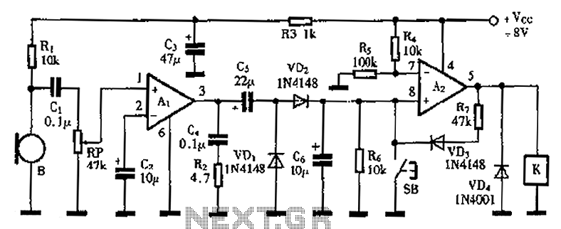
A practical voice-activated switch is presented. An A1 amplifier is connected to a conventional microphone (B) that picks up the audio control signal, which is then amplified. After amplification, the signal passes through components C5, VD1, and VD2, forming...
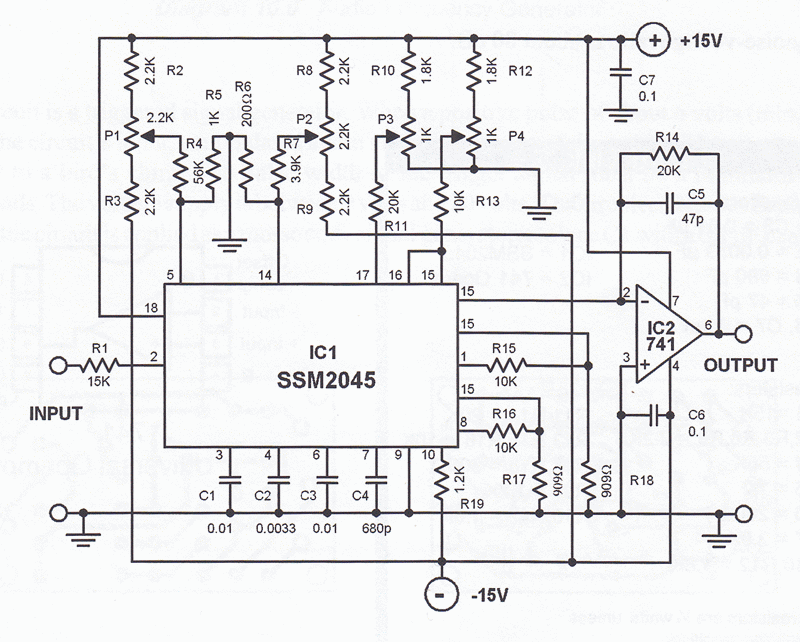
This audio processor circuit features the SSM2045 integrated circuit (IC), designed specifically for electronic music applications, along with the 741 operational amplifier (op-amp) IC. The circuit is configured as a low-pass filter with a DC voltage control for gain....

A control program typically requires more than simply turning outputs on and off; these actions are triggered by events. Such events are connected to the input of a microcontroller, which determines the subsequent actions. Inputs can originate from various...
Warning: include(partials/cookie-banner.php): Failed to open stream: Permission denied in /var/www/html/nextgr/view-circuit.php on line 713
Warning: include(): Failed opening 'partials/cookie-banner.php' for inclusion (include_path='.:/usr/share/php') in /var/www/html/nextgr/view-circuit.php on line 713