
100 Watt MOSFET Power Amplifier

Power supply for 100W amp [1]
Part List
R1=27Kohm R24=8.2ohm D1=12V 0.5W Zener R2-11=4.7Kohm R25=10ohm 1W D2.....5=8.2V 1W Zener R3-4=5.6Kohm TR1=470ohm trimmer L1=20 turns 0.6mm on R25 R5=47Kohm TR2=4.7Kohm trimmer Q1-2=BC 547 R6=1Kohm C1=1uF 63V mkt Q3=2N5460 fet R7-10-21=22Kohm C2=1nF 100V* Q4-5=MPSA93 R8=12ohm C3=100uF 16V Q6-8-11=BC182 R9=1Mohm C4=100nF 100V* Q7-10=MPSA43 R12=33ohm C5-7=22uF 16V Q9=BC212 R13-20=82ohm C6=4.7pF ceramic Q12=2SK134 or 2SK135 R14=33ohm C8=47uF 16V Q13=2SJ49 or 2SJ50 R15=2.7Kohm C9=1nF 100V* R16=270ohm C10-11=100uF 100V *polyester or mylar R17-19=680ohm C12-14=100nF 250V mkt R18=33Kohm C13=150nF 100V mkt R22-23=0.33ohm 5W C15=100uF 35V
The described circuit employs V-MOSFET technology in the output stage, providing significant advantages over traditional bipolar transistors, such as enhanced speed, thermal stability, and reduced distortion. This design incorporates several critical components and configurations to optimize performance.
The differential amplifier at the input stage is formed by transistors Q1 and Q2, where trimmer TR1 is utilized for matching the characteristics of the differential pair. The circuit uses a current source configuration involving Q3, a FET, to ensure stable operation. Current sources Q7, Q8, Q10, and Q11, based on the Wilson current mirror topology, are employed to improve output stage stability and linearity.
Biasing of the output stage is managed by trimmer TR2, allowing for precise adjustment of the bias current to approximately 100 mA, which is crucial for maintaining optimal performance and thermal management. Protection of the gate of the V-MOSFET transistors (Q12 and Q13) is achieved through the use of Zener diodes D2 to D5, which clamp the gate voltage to prevent over-voltage conditions that could damage the thin SiO2 insulation layer.
The overall gain of the amplifier is set to 32.6, adjustable through resistors R18, R6, and R8, which are part of the negative feedback loop. Local feedback mechanisms are also implemented to enhance stability across varying operational conditions. Given the positive temperature coefficient of the V-MOSFETs, the circuit design accounts for the increase in resistance with temperature, which could otherwise lead to a decrease in output current and power.
Separate power supplies for the driver and output stages are utilized to further enhance stability and minimize intermodulation distortion. The original schematic was designed by L. Hood and published in Wireless World, indicating a reputable source of inspiration for the design.
The circuit is compatible with specific V-MOSFET models, including the 2SK134 and 2SK135, as well as 2SJ49 and 2SJ50. Due to the discontinuation of these parts by Toshiba, alternative replacements such as 2SK1530 and 2SJ201 are suggested, which offer similar characteristics in a different package type.
The component list provides detailed specifications for resistors, capacitors, and other circuit elements, ensuring that builders can replicate the design accurately for a 100W amplifier application.One still designing that it uses in the exit transistor of technology V-mosfet. This transistors to us offer a lot of virtues concerning the simple bipolar transistors, as high speeds, thermic stability, low distortion etc. Beyond this circuit use also other useful solutions as use fet as source of current [ Q3 ], trimmer TR1 with which we match the characteristics of differential amplifier of entry Q1-2.
Also extensive is the use of sources of current wilson Q7-8 and Q10-11. With trimmer TR2 regulate the bias current of output stage, in the 100 ma. The use of diodes D2 until D5 in combination with the resistances R17-19, they protect the gates of transistors v-fet from exceeds the voltage ± 14V and it creates perforation in very thin layer SiO2, that is used as insulation in the gate. This way of protection is common in all the amplifiers that use these transistors. The total gain of amplifier is 32.6, regulated from the R18, R6 and R8, in the negative feedback. Also is used enough the use of local feedback for stabilisation of operation under all the conditions. Because the transistors v-fet have positive factor of temperature, with result with the increase of temperature is increased also their resistance.
This increase has as result the reduction of current that via the transistor, hence also his power. The use of separated supply in the stages of drive and exit, ensures stability and reject of distortion of intermodulation. The initial drawing of is L. Hood and was published by the Wireless Word. A branding that I want to make, that is in effect for all the amplifiers that I publish and use the POWER VMOS FET of series [ 2SK134 or 2SK135 ] [ 2SJ49 or 2SJ50 ], they are that, more above transistor they are not produced more by the Toshiba and are enough difficult they are found henceforth.
They can be replaced with [ 2SK1530 in the place of 2SK135 ] and [ 2SJ201 in the place of 2SJ50 ]. The new transistors are in plastic case ??-3? and no TO-3, bear in bigger supply of operation and have positive factor of temperature. This mean that with the increase of temperature, is increased and the current that is gone through from through the transistor. The new transistors him I have still not tryed and me it would interest to learn if somebody him used also with which results.
Power supply for 100W amp [1] Part List R1=27Kohm R24=8.2ohm D1=12V 0.5W Zener R2-11=4.7Kohm R25=10ohm 1W D2.....5=8.2V 1W Zener R3-4=5.6Kohm TR1=470ohm trimmer L1=20 turns 0.6mm on R25 R5=47Kohm TR2=4.7Kohm trimmer Q1-2=BC 547 R6=1Kohm C1=1uF 63V mkt Q3=2N5460 fet R7-10-21=22Kohm C2=1nF 100V* Q4-5=MPSA93 R8=12ohm C3=100uF 16V Q6-8-11=BC182 R9=1Mohm C4=100nF 100V* Q7-10=MPSA43 R12=33ohm C5-7=22uF 16V Q9=BC212 R13-20=82ohm C6=4.7pF ceramic Q12=2SK134 or 2SK135 R14=33ohm C8=47uF 16V Q13=2SJ49 or 2SJ50 R15=2.7Kohm C9=1nF 100V* R16=270ohm C10-11=100uF 100V *polyester or mylar R17-19=680ohm C12-14=100nF 250V mkt R18=33Kohm C13=150nF 100V mkt R22-23=0.33ohm 5W C15=100uF 35V 🔗 External reference
Related Circuits
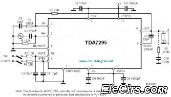
The IC TDA7295 is a monolithic integrated circuit designed for use as an audio class AB amplifier in high-fidelity applications, including home theaters and high-end televisions. The TDA7295 is a versatile audio amplifier that delivers high-quality sound reproduction, making it...
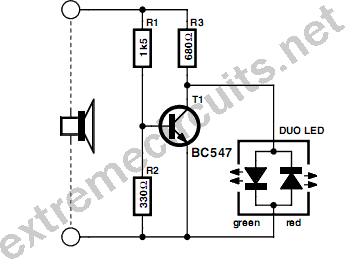
This circuit indicates the power level delivered to a loudspeaker. A dual-color LED displays green at approximately 1 watt, orange at 1.5 watts, and bright red at levels exceeding 3 watts. The circuit is connected in parallel with the...
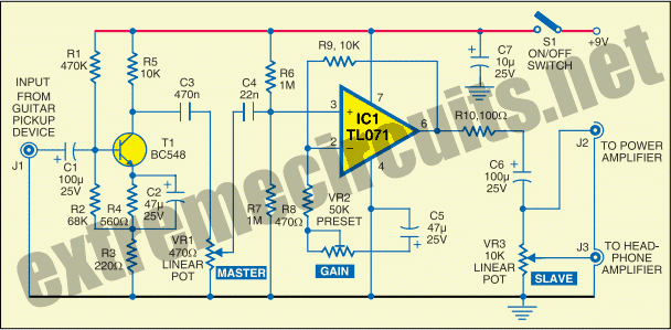
The circuit diagram of a guitar preamplifier is designed to accept any standard guitar pickup. This preamplifier is versatile, featuring two signal outputs. A typical configuration involves a pickup attached to the guitar headstock, where the pickup device consists...
I had designed up an oscillator with a Power Output circuit. Problem was when power was applied to the entire circuit, the output of the Oscillator gave a Momentary Spike into the output circuit. Thus Driving it full on...
The ICM7226 is a fully integrated Universal Counter and LED Display driver. It combines a high-frequency oscillator, a decade timebase counter, an 8-decade data counter and latches, a 7-segment decoder, digit multiplexer, and segment and digit drivers, which can...
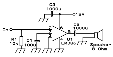
Approximately one watt RMS appears to be a suitable output level, which is also the maximum power that a basic amplifier powered by 12V can deliver to an 8 Ohm speaker. A very low saturation amplifier may reach up...