
10000Vdc Supply
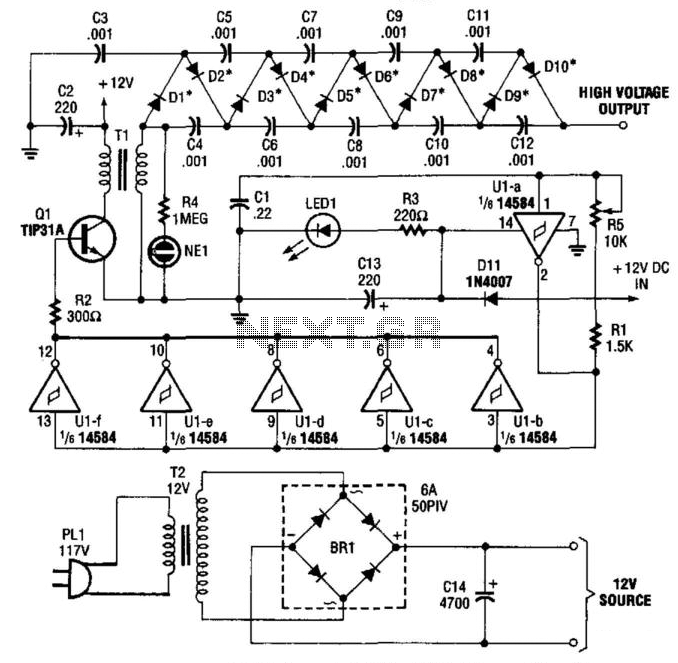
The circuit described features a CMOS oscillator (U1A) that serves as the primary frequency generator. This oscillator produces a square wave output, which is characterized by its 12-V peak-to-peak (Vpp) amplitude. The output from U1A is fed into multiple stages (U1B through U1F), which function as amplifiers or buffers to ensure the signal maintains its integrity while driving the next stage of the circuit.
The amplified square wave is then used to energize a transformer (T1). The primary winding of T1 receives the square wave input, and due to the transformer's inductive properties, it generates a higher voltage in the secondary winding. This is a critical step for applications requiring high-voltage outputs.
The output from the transformer is then directed to a rectifier-multiplier circuit composed of diodes D1 through D10, where each diode is arranged in series pairs of 1N4007. This configuration is designed to efficiently convert the alternating current (AC) square wave into a direct current (DC) voltage. The rectification process is augmented by the use of capacitors C3 through C12, which are strategically placed to smooth and store the resultant DC voltage.
The combination of the rectifier and multiplier stages allows the circuit to achieve an output voltage of approximately 10 kV. This high-voltage output is suitable for various applications, including but not limited to, high-voltage power supplies, ionization devices, and other electronic applications requiring significant voltage levels. The careful selection of components and their arrangement within the circuit ensures reliability and performance in high-voltage scenarios. A CMOS oscillator (U1A) drives. U1B through U1F, which drives Ql, which generates a 12-Vpp square wave across the primary of Tl. This square wave is applied to a rectifier-multiplier circuit consisting of Dl through D10 (each is two 1N4007 diodes in series) and C3 through C12. About 10 kV is available. 🔗 External reference
Related Circuits

A ripple-free, short-circuit protected variable output voltage and current power supply is presented on this website as a verified project. The circuit diagram includes a description of various power supply circuits. This power supply circuit is designed to provide a...
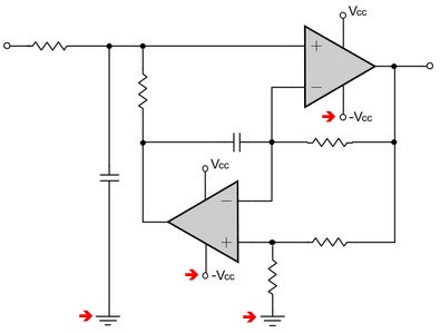
All filter stages utilizing a Virtual Ground will exhibit the Virtual Ground DC potential at their outputs, whereas all stages employing a resistive divider at their input (without a Virtual Ground) will present the divider potential at their output....
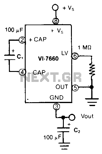
In this application, the VL-7660 is configured as a voltage splitter. The normal output pin is connected to ground, while the normal ground pin serves as the output. The switches facilitating charge pumping are bidirectional, allowing for reverse charge...
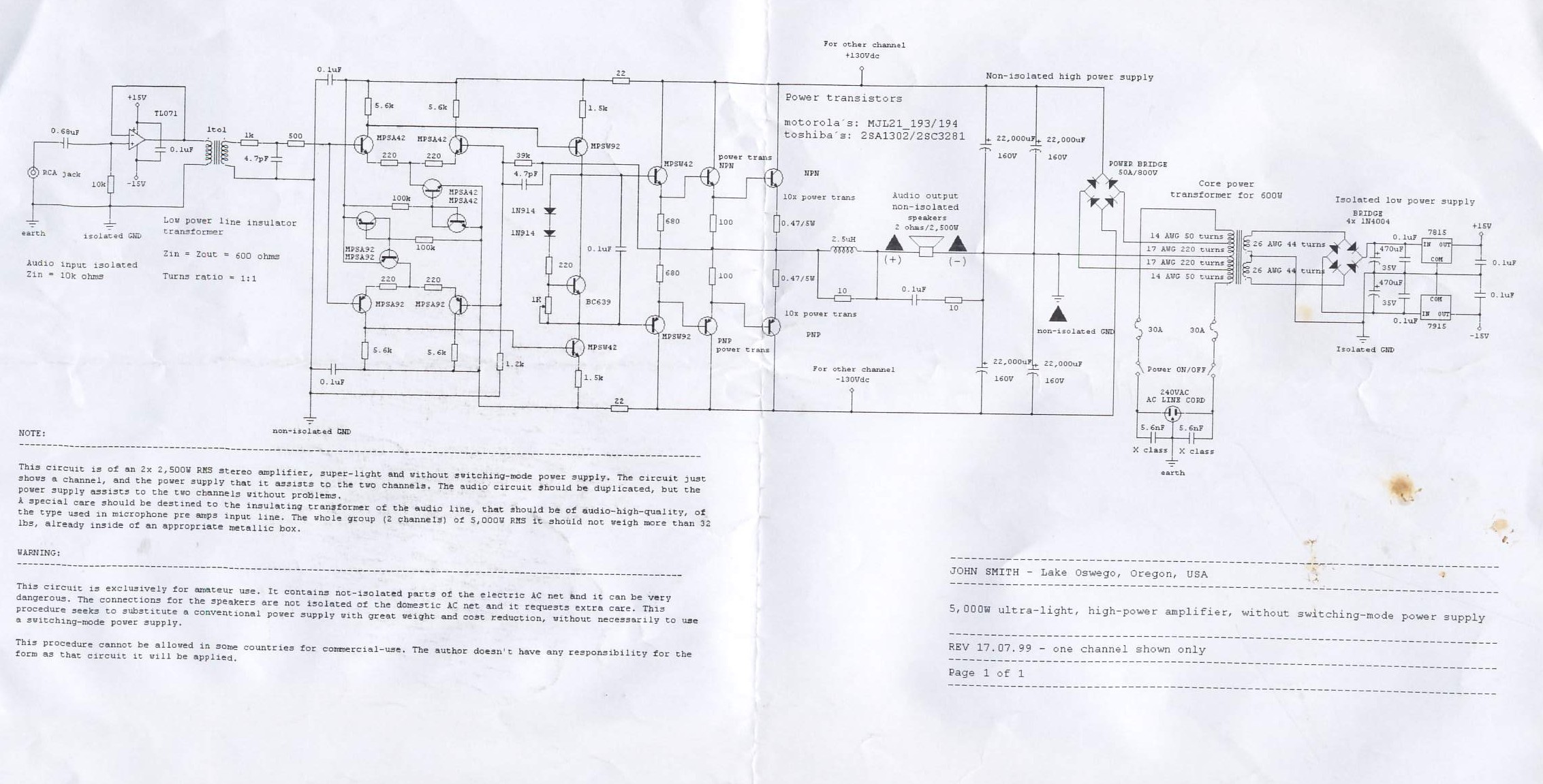
This circuit is for a 2x2, 500W RMS stereo amplifier that is super-light and does not utilize a switching-mode power supply. The circuit diagram displays only one channel, while the power supply is designed to support both channels. The...
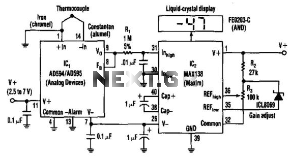
Using a J-type thermocouple, this circuit can indicate temperatures from -350° to 400° with a 6-V supply or from -50° to +100° with a 3-V lithium battery. The AD954 produces a 10 mV/°C output to the MAX 138 digital...
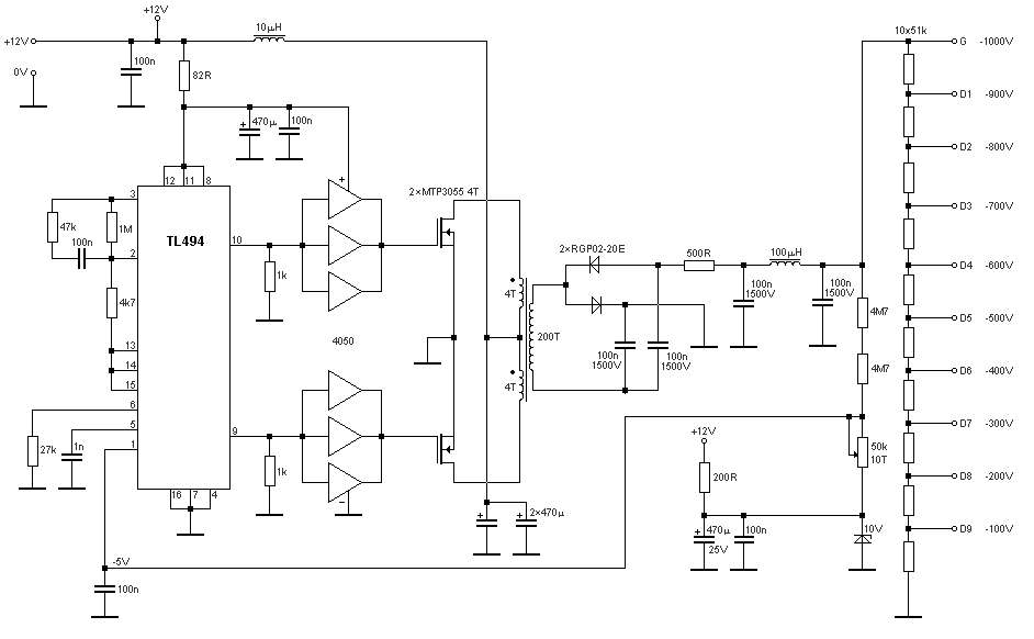
The schematic diagram originates from a circuit designed for a stable power supply ranging from -100V to -1000V. For further details, refer to the page that explains the circuit diagram associated with this power supply. This stable power supply...