
12 Volt DC Power Supply Circuit

The unit incorporates overcurrent, overtemperature, and overvoltage protections, along with passive inrush current limiting. The output ripple is approximately 0.2V peak-to-peak in the frequency range of 0 to 20 MHz. For reduced ripple, an additional output capacitor or an LC filter can be added outside of the feedback loop. This project is a modification of a 24V circuit designed previously for a small company as a plug-in replacement for a low-cost off-the-shelf AC to DC power supply. Although the design was completed and a prototype built, the company opted for an alternative supply found in stock, resulting in no further manufacturing of this module. The design has not been tested beyond basic design validation testing (DVT). The circuit can be constructed for personal use at one's own risk, but redistribution or commercial use without permission is prohibited.
For safe testing or troubleshooting, it is advised to power the circuit via an isolation transformer or from an isolated AC source. Caution is warranted as an offline single-transistor flyback converter can generate internal voltages up to 600V. Only individuals of legal age who understand power electronics and high voltage safety should attempt to work with this circuit.
The AC to DC power supply employs a flyback topology, recognized as the simplest SMPS converter design. It utilizes an 800V/11A MOSFET (Q1) as the switching device and a PWM controller (UC3844AN, U3). The input section consists of a fuse, EMI filter, an inrush current limiting NTC resistor (R1), a full bridge rectifier (CR1), and a DC bus filter capacitor (C2). Initial startup current for the PWM IC is supplied by "bleeding" resistors (R7, R8), which allow a small current to charge the Vcc capacitor (C7). When the Vcc pin of U3 reaches the positive undervoltage lockout threshold (typically 14V-16V), the IC activates, driving the switch Q1 on and off at a fixed frequency of 100 kHz.
During the on-state of Q1, the DC bus voltage is applied to the primary winding of the transformer (T1), causing the current through the primary to ramp up and energy to accumulate in the transformer's magnetic field, while diodes D4 and D7 remain reverse-biased. Upon turning off Q1, the energy stored in the magnetic field reverses the voltages across all windings, leading to conduction in output rectifiers D4 and D7, which transfers the stored energy to the output and the bias circuit. Once the converter is operational, the bias for the PWM control is derived from the bias winding of the transformer.
The secondary side feedback control loop employs a TL431 precision shunt regulator (D1) as both the reference and error amplifier, comparing the divided output voltage to D1's internal reference of 2.5V. An optocoupler (U1) transmits a current proportional to the error signal across the transformer’s galvanic isolation boundary back to the primary PWM. If precise output regulation is not necessary, feedback can be sourced from the bias voltage at capacitor C9 and fed into feedback pin 2 via a voltage divider. The primary current in T1 is monitored using a current sense resistor (R6), and the resultant voltage is applied to the control circuitry for regulation purposes.The schematic diagram below shows a simple trivial low-cost 12 volt DC 50W off-line SMPS switching power supply circuit. It can be used for DIY home projects or to learn operation of flyback converters. This PSU can work over a universal input AC line range 90-264 VAC. It provides a nominal 12V DC output at more than 4A load. Line and load regulation is better then 0. 5%. The unit has overcurrent, overtemperature and overvoltage protections, as well as passive inrush current limiting. Output ripple are approximately 0. 2 V peak to peak in the range 0 to 20 MHz. If you need to get lower ripple, you may put an additional output capacitor or an LC filter outside of the feedback loop.
This project is a modification of a 24V circuit that I`ve designed many years ago as a consultant for a small company. That company wanted a plug-in replacement to a cheap off-the-shelf AC to DC power supply, which had a long lead time.
By the time I`ve completed the design and built a proto, they found the off-the-shelf part elsewhere in stock. So, they never proceeded with a manufacturing of this module. Accordingly, I have not tested this design beyond a basic DVT. You can build this circuit for personal use (at your own risk of course). But you are not allowed to republish the content of this page anywhere or use it for commercial purposes without my permission.
To safely test or troubleshoot this circuit it is recommended to power it via an isolation transformer or from an isolated AC source. Also note that an offline single-transistor flyback converter generates internal voltages which may reach 600 V.
Don`t try to play with this circuit unless you are of a legal age, understand power electronics and know how to deal safely with high voltage. You may want to take our quick power supply safety quiz. This AC to DC power supply utilizes a flyback, which is the simplest SMPS converter topology. It uses an 800V/11A MOSFET (Q1) as the switching device and PWM controller UC3844AN (U3). The input section includes a fuse, EMI filter, inrush current limiting NTC resistor R1, a full bridge rectifier CR1, and a DC bus filter capacitor C2.
The initial start-up current for the PWM IC is provided by "bleeding" resistors R7, R8 that allow small current which charges the Vcc capacitor C7. When the Vcc pin of U3 reaches the positive undervoltage lockout threshold (typically 14V-16V), the IC starts to operate and will be driving ON and OFF the switch Q1 via a gate drive resistor R4 at a fixed frequency (in this circuit it is 100 kHz).
When Q1 turns on, the DC bus voltage is applied across the transformer T1 primary winding, current through the transformer primary ramps up and energy is accumulated in the transformer`s magnetic field. Diodes D4 and D7 during this time interval are reversed biased. When Q1 turns off, the energy stored in the magnetic field causes the voltages across all winding to reverse polarity.
As a result, output rectifiers D4 and D7 conduct and the stored energy is transferred to the output and to the bias circuit. Once the converter is started, the bias for the control PWM comes from the bias winding of the transformer.
The secondary side feedback control loop uses a TL431 precision shunt regulator D1 as both the reference and an error amplifier. It compares divided output voltage to D1`s internal reference 2. 5V. An optocoupler U1 feeds the current proportional to the error signal across the transformer galvanic isolation boundary back to the primary PWM.
If accurate regulation of the output is not required, the feedback can be taken from the bias voltage at C9 and fed via a divider into feedback pin 2. Primary current in T1 is sensed by a resistor R6. This current sense voltage is applied th 🔗 External reference
Related Circuits
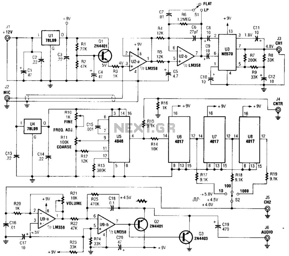
The precision audio frequency generator consists of several sub-circuits: an audio amplifier/filter circuit, an automatic level control, a variable voltage-controlled oscillator, a frequency divider circuit, an integrator, and an audio output amplifier. An electret microphone element is utilized to...
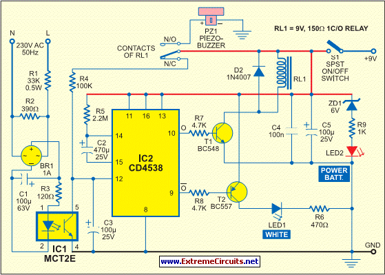
This circuit alerts users with an alarm whenever the AC mains supply fails. It also provides a backup light to assist in locating a torch or generator key in the dark. The circuit is powered by a 9V PP3/6F22...
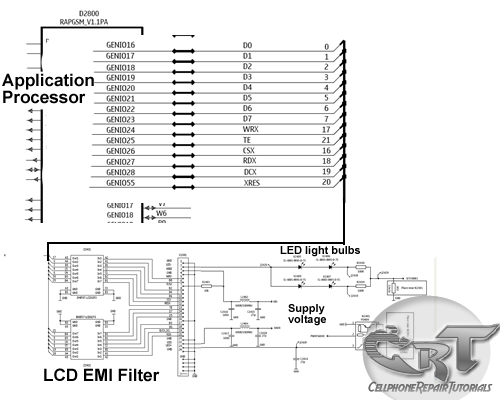
An LCD (liquid crystal display) is an electronically modulated optical device composed of multiple pixels filled with liquid crystals, arranged in front of a light source (backlight) or reflector to create images in color or monochrome. The block diagram...
Arcing completes a circuit -- closes a system -- between two voltage potentials. When arcing occurs, two oppositely charged static voltage potentials can cancel each other out. The arcing problems that occur are usually between two electrically isolated voltage...
A circuit diagram of the T1 is a low-impedance output transformer, featuring a 5000-8 ohm resistor. The T1 low-impedance output transformer is designed to match the output of audio amplifiers to the impedance of loudspeakers, ensuring optimal power transfer and...
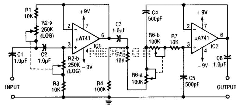
This circuit is a variable audio bandpass filter that features a low cutoff adjustable from approximately 25 Hz to 700 Hz and a high cutoff adjustable from 2.5 kHz to over 20 kHz. The roll-off is set at 12...