
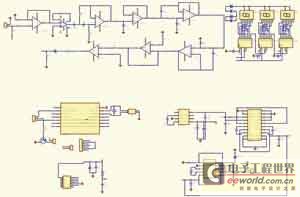
15V And 5V Car Battery Supply
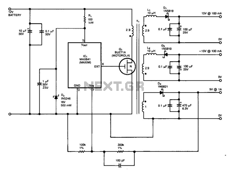
IC1 operates as a high-frequency switching regulator, producing a 45-kHz square wave that controls the gate of MOSFET Q1. The use of Schottky diodes D1, D2, and D3 is critical due to their low forward voltage drop and fast switching characteristics, which enhance the overall efficiency of the circuit. The regulator maintains a stable 5-V output by utilizing feedback from the output voltage to modulate the gate signal of Q1. When the output voltage exceeds the 5 V threshold, the feedback mechanism effectively turns off the gate drive, preventing overvoltage conditions.
Transformer T1 is designed with trifilar windings, which provide the necessary isolation and voltage transformation while ensuring minimal coupling losses. The 2% regulation capability indicates that the output voltage remains stable despite variations in load current, making it suitable for applications with fluctuating power demands. The primary inductance of approximately 21 µH is optimized for the switching frequency, ensuring adequate energy transfer during each switching cycle.
The core of transformer T1 must be adequately sized to handle peak currents of 4 A without saturating, which is essential for maintaining performance under load. The specified turn ratios—11.5 turns for each 15-V output, 11.5 turns for the primary, and four turns for the 5-V secondary—are designed to achieve the desired output voltages from the input supply while ensuring efficient energy conversion.
Overall, the circuit achieves an efficiency of around 75%, indicating that a significant portion of the input power is converted to usable output power, with minimal losses attributed to heat and other factors. This design is well-suited for applications requiring reliable voltage regulation with efficient power management. IC1 is a switching regulator that generates a 45-kHz signal that drives the gate of MOSFET Ql. Dl, D2, an d D3 are Schottky diodes. The 5-V output is sensed as a reference; feedback to the chip turns off the gate signal to Ql if the voltage rises above 5 V. Tl has Trifilar windings that assume about 2% regulation for a 10-to 100-mA load change on the ± 15-V supplies.
R1/D4 provide overvoltage protection. Tl has a primary inductance of about 21 . Core size should allow 4-A peak currents. The turn ratios are IIV2 turns each for the 15-V supplies, ll1/2 turns for the primary, and four turns for the 5-V secondary. The efficiency is about 75%. 🔗 External reference
Related Circuits
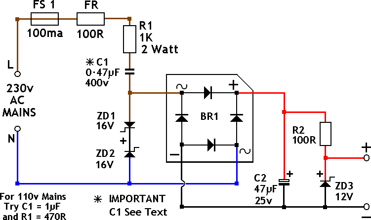
This circuit will supply up to approximately 20 mA at 12 volts. It utilizes capacitive reactance instead of resistance and does not generate significant heat. The described circuit operates as a capacitive power supply, which is an efficient method to...
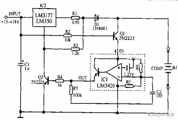
A lithium-ion battery charging circuit is illustrated above. Initially, when charging begins, if the battery voltage is below 8.4V, the output of IC1 is inactive. As a result, Q2 remains off, and the LM317 operates in constant current mode....
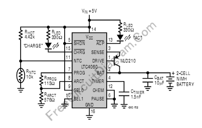
This simple battery charger circuit is designed for NiMH/NiCd batteries. It requires no microcontroller or any programming. Linear Technology Corporation. The described battery charger circuit is intended for use with nickel-metal hydride (NiMH) and nickel-cadmium (NiCd) batteries, which are commonly...
A walkie cardiotachometer has been designed to replace the traditional method of measuring heart rate using a pulse auscultator. This device is user-friendly and consists of three main components: signal collection, data processing, and an LED display along with...
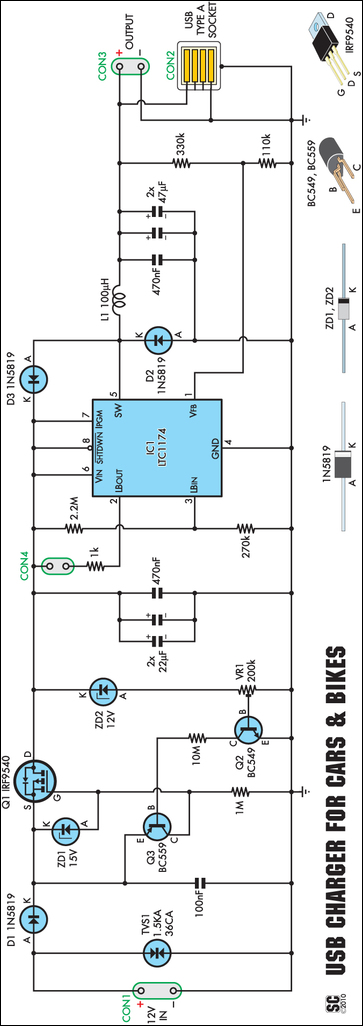
A regular charger was tested and found to consume 13mA with no load. It features an integrated power LED, which significantly contributes to standby current consumption. However, since the cigarette lighter socket is powered only when the engine is...
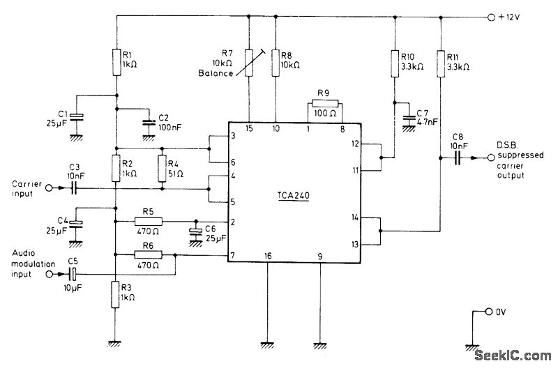
The Mullard TCA240 is a dual balanced modulator-demodulator that effectively suppresses the carrier frequency at the output, which is essential for Single Sideband (SSB) or Double Sideband (DSB) operation in transmitters. The bias resistor R7 is adjustable to achieve...