
16 Step Sequencer
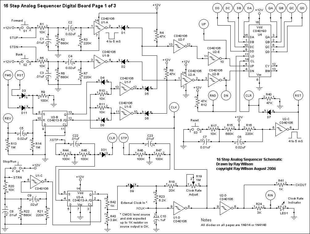
The described circuit involves several critical components and their interconnections, forming a sequencer clocking mechanism. The U4 counter serves as the core element for counting steps, with its functionality heavily reliant on the proper configuration of inputs and the associated logic gates. The design incorporates debouncing techniques for switches to ensure clean transitions, preventing erratic behavior during operation. The clock generation section, utilizing a Schmidt trigger inverter, is designed for stability and reliability, ensuring that the sequencer operates smoothly under various conditions. The integration of external clocking capabilities reflects a versatile design approach, allowing the sequencer to synchronize with other devices while accommodating different signal levels. The detailed connections and component values are crucial for achieving the desired performance, and understanding the operation of each section is essential for successful implementation. The overall schematic design emphasizes modularity and adaptability, making it suitable for integration into larger synthesizer systems or standalone applications. Proper assembly and testing of the circuit will require adherence to best practices in electronics, including careful soldering, signal integrity checks, and thorough troubleshooting to resolve any potential issues during the initial setup and operation phases.an intermediate to advanced project and I do not recommend it as a first project if you are just getting started in synths or electronics. Only the circuit and some explanation are shown here. A lot of project building, troubleshooting and electronics experience is assumed. Additionally, electronic equipment ownership (scope, meters, etc. ) is taken for granted. If you are interested in building this project please read the entire page before ordering PC boards to ensure that the information provided is thorough enough for you to complete the project successfully. Page 1 shows the clocking and counting section of the circuit. This part of the circuit controls the manual and automatic stepping of the sequencer. U4 counts up when a positive going edge is applied to its UP input while its DN input is held high. Conversely it counts down when a positive going edge is applied to its DN input while the UP input is held high.
If the LD input is brought low the outputs of U4 (QA through QD) follow the data on the load inputs (DA through DD). When the sequencer is not in Random mode the LD input is held high via R12 to +12V. A high level on the CL input of U4 causes the counter to reset to a count of zero. S1 and associated components (R1, C2, C1, R2, R3, and U1-A) comprise a switch debouncer/low going pulser.
When S1 is pressed a clean low going pulse of about 1 to 2 mS appears at the output of U1-A. In the same manner, S2 and its associated components and S4 and its associated components form switch debouncer/low going pulsers. S3 and its associated components work in the opposite fashion of S1, S2 and S4 in that when S3 is pressed a clean positive going pulse appears at U2-C pin 6.
S3 is used soley to reset counter U4. The clock (square wave oscillator) for the sequencer is made up of U1-D, C10, R23, R18, and R19 (clock rate adjust). It runs when U3-A`s Q output is low thus reverse biasing D9. Due to U1-D being a schmidt trigger inverter it can be made to oscillate by applying its output back to its input via a resistor and connecting a capacitor to its input.
When the output is high it charges C10 via R19, R18, and R23 in series until its high threshold is reached at which time its output snaps low and C10 discharges through the same path until U1-D`s low threshold is reached when its output snaps high and begins the cycle anew. The purpose of the value changes needed for the clock input modification is to raise the impedance of the external clock input node so that external clocking from sources with output impedance up to 1K can reliably clock the sequencer.
A clean rectangular clock source oscillating between ground and +V is assumed. If an external clock source with negative voltage excursions is used then a diode must be placed between the input jack and pin 9 of U1-D. The anode of the diode goes to the jack`s hot and the cathode goes to pin 9 of U1-D. If U3-A`s Q output is high the clock is stopped (due to C10 being held fully charged via D9) and its output (U1-D pin 8) is forced low.
Pressing S4 toggles the state of U3-A`s Q output since U3-A is wired as a divide by two counter. Thus you can start or stop the clock by pressing S4. The clock signal is fed to the inputs of U1-F and U1-E via 10K resistors R10 and R11 respectively. D4 and D5 are used (in conjunction with U3-B) to control which of these inverters propogate the clock signal. U3-B is used to control the direction in which U4 counts. When the clock is running and U3-B`s Q is high (and subsequently its NOT-Q is low) the clock pulses are allowed to propogate through U1-F but are stopped from passing through U1-E due to U1-E`s pin 11 being pulled low via D8.
When the clock is running and U3-B`s Q is low (and subsequently its NOT-Q is high) the clock pulses are allowed to propogate through U1-E but are stopped from passing through U1-F due to U1-F`s pin 13 being pulled low via D4. Notice that the an 🔗 External reference
Related Circuits
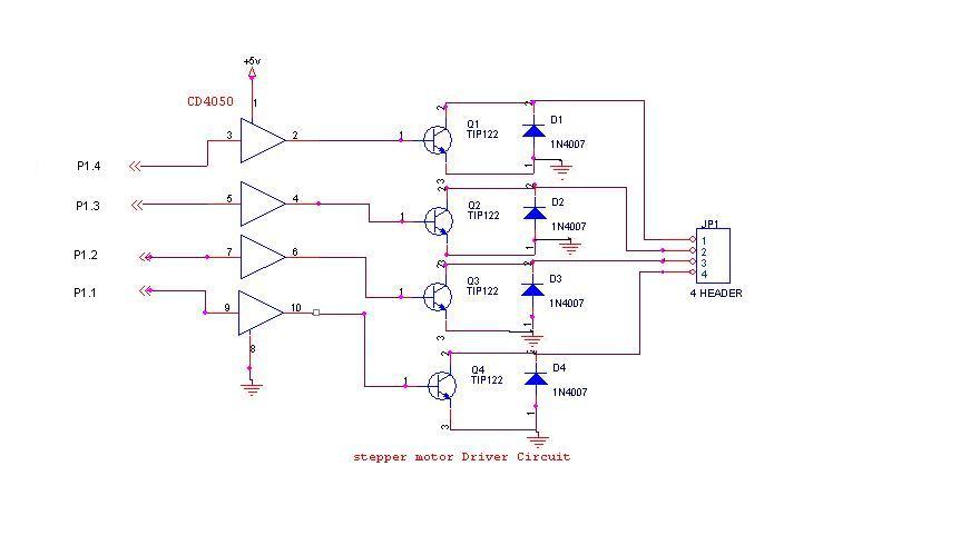
A 6V, 2A stepper motor is utilized in this circuit. The CD4050 hex buffer is employed to connect to the microcontroller. The output of the CD4050 is linked to the base of a TIP122 transistor. The emitter and collector...
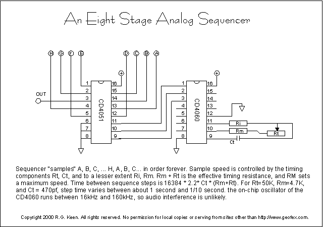
The CD4060 is a CMOS 14-stage binary counter with an internal oscillator on chip. The oscillator is controlled by the resistors and capacitor tied to the timing pins, 9-11. This oscillator runs the binary counter, and the various outputs...
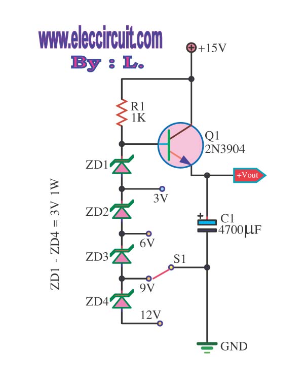
This is a DC regulator circuit that can provide multiple output voltages simply. It functions as a simple step-down DC converter and is designed with a fixed resistor R1. The described circuit operates as a DC voltage regulator, specifically designed...
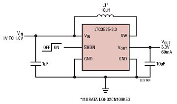
The LTC3525-3/LTC3525-3.3/LTC3525-5 are high-efficiency synchronous step-up DC/DC converters with output disconnect capability that can operate with an input voltage as low as 1V. These converters provide a compact and efficient alternative to charge pumps for single-cell or dual-cell alkaline...
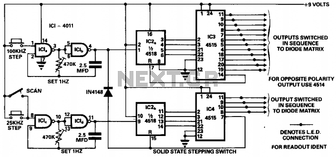
This circuit was designed to ensure safe operation of a 48-channel mobile transceiver while in motion. It incorporates oscillators that facilitate single-stepping or scanning functions. The scanning feature enables the user to sequentially check all 48 channels for occupancy,...
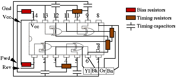
The NuStepper is a circuit designed by Wilf Rigter, utilizing a 74AC86 quad XOR chip to create four neural neurons configured in a ring. This circuit operates similarly to a microcore and can drive a bipolar stepper motor. The...
Warning: include(partials/cookie-banner.php): Failed to open stream: Permission denied in /var/www/html/nextgr/view-circuit.php on line 713
Warning: include(): Failed opening 'partials/cookie-banner.php' for inclusion (include_path='.:/usr/share/php') in /var/www/html/nextgr/view-circuit.php on line 713