
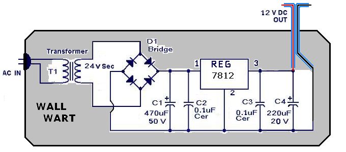
1880MHz internal bias circuit diagram of the amplifier application collector RF2324
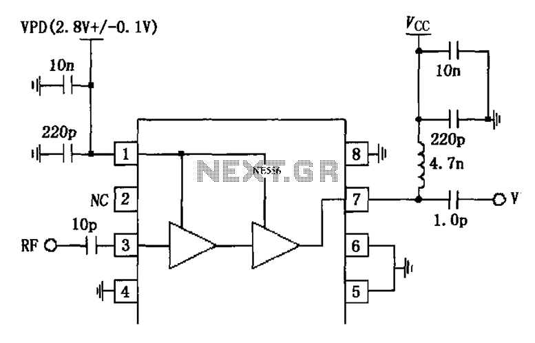
The RF2324 amplifier circuit operates at a frequency of 1880MHz, primarily used in wireless communication applications. The RF signal enters through pin 3, where it is initially amplified by a preamplifier stage. This preamplification is crucial for enhancing the weak RF signals to a level suitable for further processing. The term "7 feet" refers to the distance or the layout of the circuit traces, which can influence the signal integrity and performance due to parasitic capacitance and inductance.
The internal amplifier is coupled with a 10pF capacitor, which is strategically placed to block any DC components while allowing the RF signal to pass through. This coupling capacitor is essential in maintaining the desired signal characteristics while preventing DC bias from affecting the amplifier's operation. Impedance matching at 50 ohms is critical in RF circuits to minimize signal reflections and maximize power transfer, which is achieved through careful design of the external output matching network.
The open collector output terminal, referred to as "7 feet," can connect to a power supply (Vcc) through either a choke or a matching inductor. This connection aids in stabilizing the voltage supply and filtering out unwanted noise. The external output matching network is designed to ensure that the amplifier's output impedance aligns with the system's requirements, optimizing both output power and efficiency.
The power-down control terminal, indicated as "1 foot," allows for the circuit to be turned off when not in use, thereby conserving power. The specified voltage levels for VPD are critical for the operation of the circuit; a voltage of 2.8V ± 0.1V keeps the circuit active, while a drop to 0.9V effectively disables it. The need for an additional RF bypass circuit for VPD indicates that further filtering may be necessary to ensure stable operation and prevent unwanted oscillations or noise from affecting the amplifier's performance. Overall, this circuit design exemplifies careful consideration of RF principles to achieve reliable and efficient amplification in communication systems. As shown in FIG constituted by RF2324 1880MHz internal amplifier collector bias application circuit. Radio frequency (RF) signal from the input pin 3, via a preamplifier, after the last stage power amplifier output is amplified by 7 feet. 3 feet directly coupled to the internal amplifier, thus blocking plus a 10pF of capacitance coupling, impedance matching at 1880MHz work to 50. 7 feet for the open collector output terminal can be connected to the power supply Vcc through choke or matching inductor, the pin impedance matching is typically 50, external output matching network allows the amplifier output impedance matching for maximum output power and efficiency.
1 foot for the power down control terminal. When VPD 2.8V 0.1V when (IPD is typically 8.5mA) circuit; when VPD 0.9V circuit closes. VPD requested additional RF bypass circuit.
Related Circuits
The AC input circuit functions as a converter, transforming an alternating current (AC) signal into a direct current (DC) signal, which is subsequently processed by an analog-to-digital (A/D) converter chip. The input circuit is designed to handle AC signals, typically...
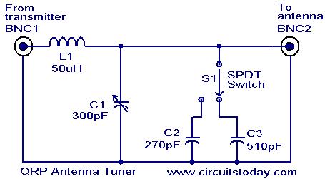
Low power (3 to 30 MHz) transmitters constructed by amateur radio operators are commonly referred to as QRP transmitters. A well-tuned antenna is essential for these transmitters; if the impedance is not properly matched, the output will be minimal...
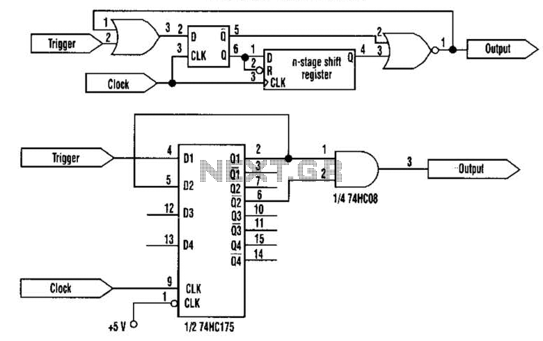
This approach utilizes a Hip-Hop, a shift register, and two gates (A). Before the one-shot pulse, the output of the NOR gate is 0. Consequently, the data input of the D-type flip-flop is equivalent to the trigger. When a...
A distortion circuit is being developed utilizing a single 12AU7 tube configured as a diode. The design is acknowledged as basic, intended primarily for the purpose of adding distortion effects. The proposed circuit leverages the 12AU7 vacuum tube, which is...
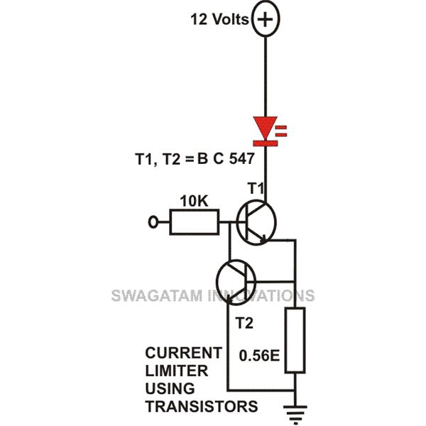
This article compiles small transistor circuits and configurations suitable for beginners, including current amplifiers, limiters, oscillators, and latches. A simple current amplifier circuit can be constructed using just a couple of NPN transistors. Additionally, two transistors and resistors can...
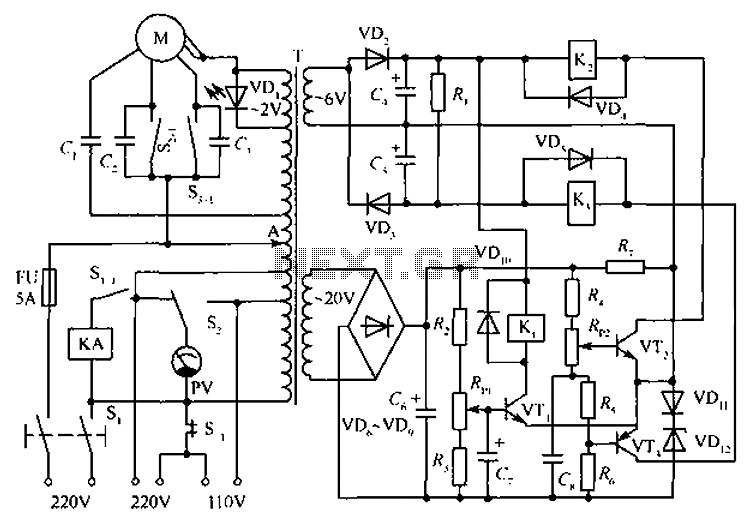
The circuit depicted in the figure includes an automatic voltage regulator (T) that maintains a constant output by utilizing a servo motor. The circuit features transistors VT1 and VT2 (3DK9), with a capacitance range of C (65 ~ 85)....