
1kHz square wave signal source circuit

The 1 kHz square wave signal source circuit utilizes the CD4060, a versatile CMOS IC that integrates a high-frequency oscillator with a binary counter. The circuit configuration begins with the connection of an external crystal oscillator, which sets the base frequency for the system. The crystal is selected based on the desired output frequency, and its stability ensures accurate frequency generation.
The feedback resistor R1 plays a crucial role in defining the gain and stability of the oscillator. By adjusting R1, the operating point of the internal gate can be optimized, allowing for reliable oscillation. Capacitor C2 is employed for frequency adjustment, enabling precise tuning of the oscillation frequency. This is particularly important when aiming to achieve specific output frequencies, as slight variations in capacitance can lead to significant changes in frequency.
The CD4060 features an internal frequency divider, which divides the high-frequency output signal. In this case, the output from the oscillator is 4.096 MHz, and the division factor of 4096 results in a final output frequency of 1 kHz. This division is accomplished through the binary counting mechanism within the IC, which allows for the generation of lower frequencies from a higher input frequency.
The output signal is available at pin 3 of the CD4060, providing a square wave that can be used in various applications, including clock generation for digital circuits, signal modulation, and waveform generation. The square wave output is characterized by its fast rise and fall times, making it suitable for driving other digital logic circuits.
Overall, the 1 kHz square wave signal source circuit using the CD4060 is a robust solution for generating precise timing signals in electronic applications, leveraging the capabilities of the integrated circuit to achieve reliable performance.1kHz square wave signal source circuit Illustrated is a use CD4060 composed of standard square wave signal source circuit. CD4060 ? foot, foot crystal rr external and compensat ion capacitor cl, c2, etc. with internal chip oscillator crystal oscillator circuit, wherein R, is the feedback resistor to determine CD4060 internal operating point gate. C2 is the frequency adjusting capacitor, the oscillation frequency can be adjusted cZ adjusted to the exact value.
The oscillation signal by the IC internal level to put large, the direct (1/4096) divided by a fixed frequency divider Lc inside, and from the IC output pin O O feet, so from the resulting output frequency rate of 4.096 MIh/4096 1 kHz. foot signal output from the output frequency of 4.096 MHz.
Related Circuits
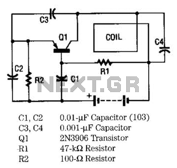
The metal locator utilizes a one-transistor oscillator in conjunction with an AM radio to detect metal. Transistor Q1 is a PNP transistor connected to the oscillator circuit. Resistor R1 supplies the appropriate base bias, while capacitors C3 and C4,...
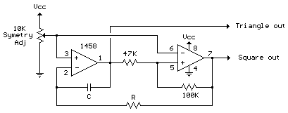
A simple triangle and square wave generator utilizing a common 1458 dual op-amp, capable of operating from very low frequencies up to approximately 10 kHz. The time interval for one half-cycle is determined by the product of resistance (R)...
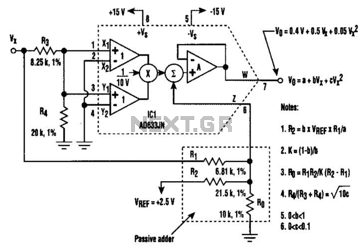
A circuit utilizing a single analog multiplier and five precision resistors can produce an output voltage (Ko) that represents a second-order polynomial. This circuit implements the quadratic function. The input terminals of IC1 are configured to create a positive...
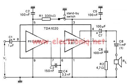
The TDA1020 is a monolithic integrated 12 W audio amplifier housed in a 9-lead single in-line (SIL) plastic package. Although it is designed primarily for car audio applications, it can also be utilized in various other audio applications. The TDA1020...
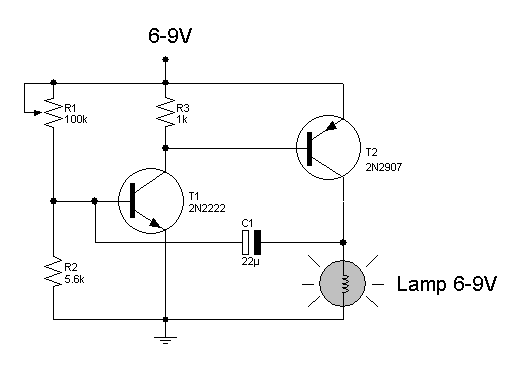
Light flashing circuit. This circuit is designed to create a small lamp that flashes with a signal at a rate of one flash per second, controlled by adjusting the lamp voltage through resistor R1. The rate is adjustable to...
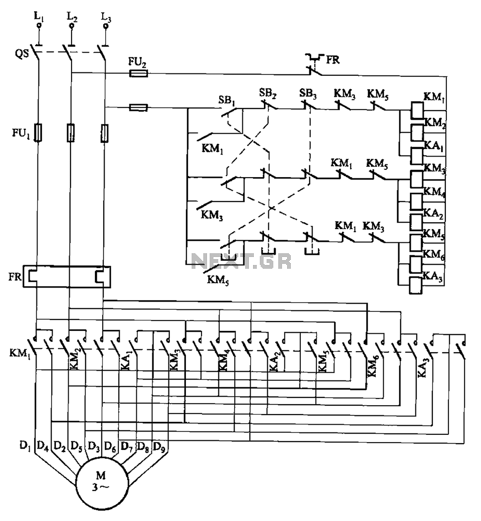
The circuit depicted in Figure 3-115 utilizes contactors and double buttons, allowing for speed conversion without the need to press the stop button. The buttons SBi, SBz, and SB3 correspond to high, medium, and low-speed operation, respectively. This circuit design...