
27MHz remote control
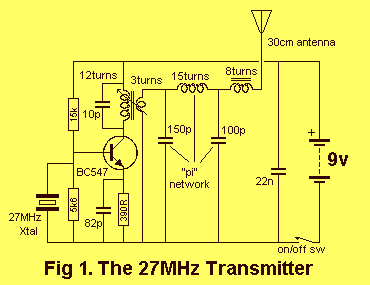

The described circuit functions as a simple crystal oscillator transmitter and receiver system. The transmitter operates primarily using a crystal oscillator that is stabilized by a tuned circuit comprising a transformer and a capacitor. The oscillator generates a frequency that is maintained by the crystal, ensuring consistent output even with variations in temperature and supply voltage. The transistor amplifies the signal, and the transformer provides impedance matching between the high-impedance output of the transistor and the low-impedance antenna.
The transformer’s turns ratio is critical, with the primary winding designed with approximately 12 turns and the secondary with about 3 turns, facilitating effective signal transfer. A pi network further refines the impedance matching to ensure optimal energy transfer to the antenna. The super-regenerative receiver design is characterized by its sensitivity to incoming signals, allowing it to detect weak transmissions. The receiver amplifies any detected signal variations, which are processed through multiple stages, including filtering to eliminate high-frequency noise components.
The use of capacitors and resistors in both transmitter and receiver circuits plays a vital role in establishing the operating conditions, biasing, and signal processing. The electrolytic capacitors specifically help manage timing and stability within the receiver, allowing it to differentiate between noise and actual signals. Overall, this circuit exemplifies a fundamental approach to RF transmission and reception, utilizing basic components to achieve effective communication.The transmitter is a very simple crystal oscillator. The heart of the circuit is the tuned circuit consisting of the primary of the transformer and a 10p capacitor. These two components oscillate when a voltage is applied to them. The frequency is adjusted by a ferrite slug in the centre of the coil until it is exactly the same as the crystal.
The crystal will then maintain the frequency over a wide range of temperature and supply voltage fluctuations. The transistor is configured as a common emitter amplifier. It has a resistor on the emitter for biasing purposes but the 82p across the 390R effectively takes the emitter to the negative rail as far as the signal is concerned.
The crystal has a fundamental of about 9MHz and it will oscillate at this frequency unless assisted to oscillate at a higher frequency. This is done by the tuned circuit oscillating at 27MHz. Now we will look at the impedance-matching feature of the transformer. The impedance of the output of the transistor is about 1k to 5k and this means it is the impedance (resistance) "it works at." In other words, it is the characteristic impedance of the transistor in this type of stage.
The impedance of a whip antenna is about 50 ohms and the transformer matches these two by having a TURNS RATIO. The primary has about 12 turns and the secondary about 3 turns. This provides part of the matching requirement. The `pi' network, made up of the 150p, 15 turn air-cored coil and 100p capacitor assists further in matching the output of the transformer to the antenna.
When the power is applied, the transistor turns on fairly hard due to the 82p in the emitter being uncharged. This puts a pulse of energy through the 10p and as the transistor turns off slightly due to the 82p charging, the energy in the 10p capacitor is passed to the primary of the transformer to start the 27MHz cycle.
The action of the emitter rising and falling during start-up, allows the base to rise and fall and this puts a pulse on the crystal to start it oscillating. The frequency of oscillation OF THE CIRCUIT is generated by the tuned circuit in the primary of the transformer and the crystal merely keeps the circuit operating at exactly 27.145MHz (or 27.240MHz, depending on the frequency of the crystal).
The turns ratio of the transformer converts a high voltage waveform (that has little current) from the transistor, into a low voltage waveform with a higher current. This is exactly what the antenna requires. But before the signal passes into the antenna it goes through the pi network, then an 8 turn Radio Frequency Choke.
This is 8 turns of enamelled wire wound on a ferrite core and is called a base-load for the antenna. The result is a 27MHz frequency called a CARRIER. The carrier produces a clean spot on the band that is free from background noise. HOW THE RECEIVER WORKS The first thing you have to realize is the receiver is really a transmitter. It's a very weak transmitter and delivers a low level signal to the surroundings via the antenna. When another signal (from the transmitter) comes in contact with the transmission from the receiver it creates an interference pattern that reflects down the antenna and into the first stage of the receiver.
The receiver is a super-regenerative design. This means it is self-oscillating (or already oscillating) and makes it very sensitive to nearby signals. It is much more sensitive than receiving a signal and making it oscillate a transistor. A super-regenerative design is not universally used because it is much more noisy than conventional reception and is not suitable for voice transmission.
However it is used in simple walkie-talkies and this is why they are so noisy - as will be shown at the end of this article. When a signal of the same frequency as the super-regenerative circuit passes near the antenna, the circuit has difficulty radiating a signal.
This means the circuit current VARIES. These variations appear across the 2k2 load resistor as a change in voltage and the signal is picked off via a 100n capacitor and passed to the second and third stages for amplification. The 22n across the first stage is designed to remove the high-frequency component from the waveform. If this were not present, the circuit would never change state. The receiver is tuned to the frequency of the crystal in the transmitter via a slug-tuned coil in the collector.
When the transmitter is off, the receiver picks up background noise and amplifies it to produce random-noise. This is amplified by the second transistor and passed to the third via a 0.47u electrolytic. This electrolytic is designed to keep the third transistor ON for the major part of the time and it does this in a very clever way.
We will assume the supply has just been turned on and the second transistor is not receiving a signal. The 0.47u will be uncharged and it will charge via the 10k collector resistor and the base-emitter junction of the third transistor.
The action of the current flowing through the base of the third transistor will turn it ON but after a short time the electrolytic will be fully charged and the current will cease and the transistor will turn off. A 10u on the collector of the third transistor will then begin to charge via the 2k2 resistor and after a period of time called the DELAY TIME, the output will be HIGH and change the state of the bridge.
But if a signal is present on the collector of the second transistor, (in our case this will be background hash), the voltage on the collector will be rising and falling. When the voltage goes low, it takes the positive end of the 0.47u low and the other end must follow. The voltage on the negative end will go below the negative rail and at -0.7v it gets clamped by the diode.
This means the electrolytic gets discharged very rapidly when the second transistor turns on. The result is the electrolytic takes a long time to charge and a short time to discharge, even when random noise (hash) is being processed. 🔗 External reference
Related Circuits

This project entitled Remote Control Through Internet allows us to monitor, control and automate our home from remote locations. In existing system home automation and security are separate systems working independently. Also in existing system if any one of...
Here is a teleremote circuit which enables switching on and off of appliances through telephone lines. It can be used to switch appliances from any distance, overcoming the limited range of infrared and radio remote controls. The circuit described...

The LK16-5/31 type master controller and PQY2 Series Magnetic control panel comprise a control circuit. The PQY2 series control panel, along with the magnetic PQY1 control panel, features a similar control circuit. The electrical components are fundamentally the same;...

The Wildcard requires a minimum of 8 volts on the V+Raw power rail, which must not exceed 26 volts. When using the Docking Panel or Power Dock, the V+Raw rail is automatically connected. If not using a dock, manual...
It was one of those days when learning chemistry, philosophy, and literature seemed necessary. Contemplating my plans for the day, I decided to embark on a project that I had wanted to undertake for a long time but had...
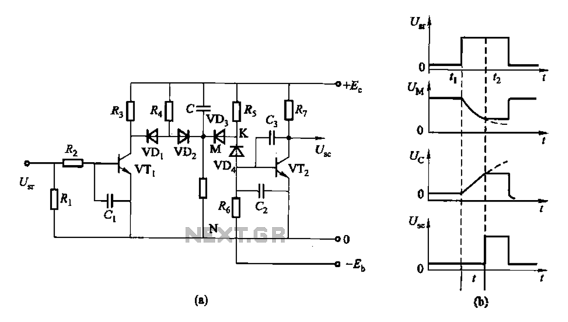
This is a control rechargeable delay circuit. Under normal circumstances, when there is no input signal, the transistor VTi is off. VTz is conducting, resulting in a low output potential (U). When a signal is applied, VTi turns on,...