
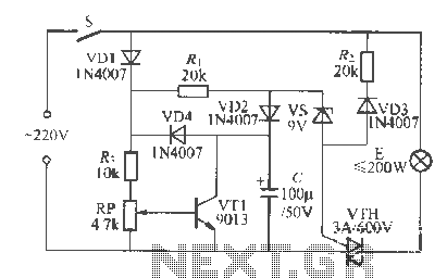
As of control rechargeable delay circuit
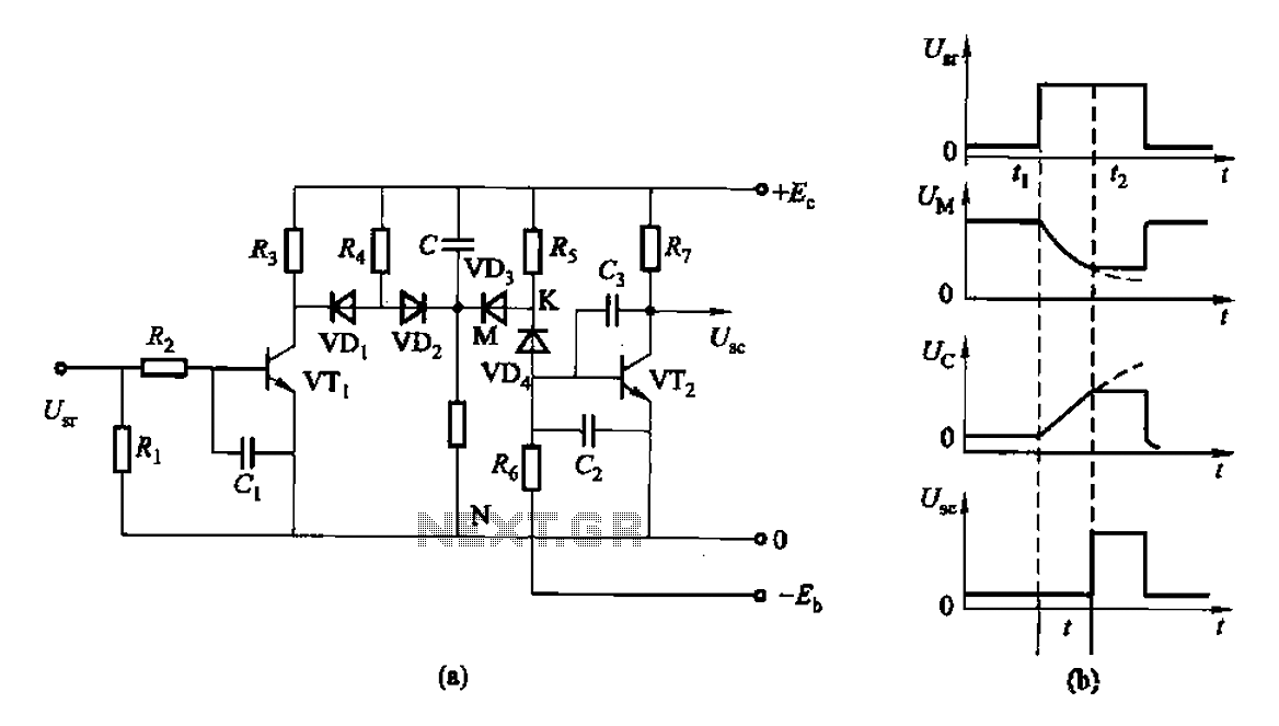
The control rechargeable delay circuit operates effectively by utilizing two transistors, VTi and VTz, to manage the signal input and output states. In the absence of an input signal, VTi remains in the off state, allowing VTz to conduct. This configuration ensures that the output voltage (U) is maintained at a low level, effectively grounding the output.
Upon receiving an input signal, VTi switches to the on state, which simultaneously turns off VTz. This transition causes the output voltage (Us) to rise to a high potential, indicating the presence of the input signal. The circuit's behavior is governed by the timing characteristics defined by the RC time constant, which is influenced by the resistive (R) and capacitive (C) components within the circuit.
The delay period during which the output remains high after the input signal is removed is determined by the equation t = RC ln(Vs/V). This relationship illustrates how the time delay is affected by the ratio of the regulator voltage (Vs) to the voltage across the components (V). The stability of the time characteristics is enhanced when the condition UMW/E = -0.37 is met, leading to a more predictable and reliable output response.
In practical applications, this delay circuit can be employed in various electronic systems where timed responses to input signals are critical. Its design allows for flexibility in adjusting the timing characteristics through the selection of appropriate resistor and capacitor values, enabling it to meet specific operational requirements in control systems, timers, and other electronic devices.As of control rechargeable delay circuit Under normal circumstances, when there is no input signal, the transistor VTi off. VTz conduction, the output U. Low potential. When U. , So that the signal voltage VTi turned, VTz off, the output Us. High potential. When Ua, signal disappears, VTi off, VTZ conduction, U.. He reverted to the low potential. From U. The signal appears to U ;. It goes high for the time interval delay circuit at the time. can be calculated as follows: z RCln poison (s) where U MN- regulator vs becomes turned off by the M, the voltage between N, V. When UMW/E. -0. 37 when, t-RC, time characteristics more stable, and can be the most time-lapse t...
Related Circuits
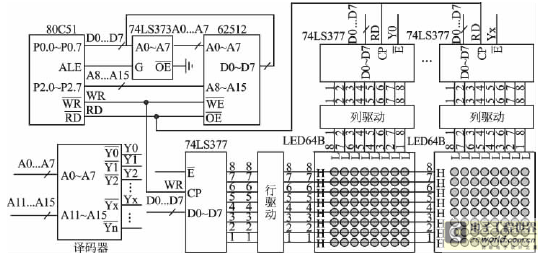
This document outlines the theory behind a high-speed control scheme for an LED display screen circuit. The circuit utilizes the MCS51 series microcontroller to manage the LED display. A 62512 random access memory (RAM) is employed for data storage,...
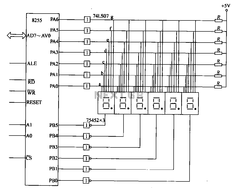
This circuit demonstrates a typical six-digit dynamic display configuration. It utilizes the PA 8255 for display output code and the PB port for bit selection code. The display buffer is designated as DISBUF, which processes the hexadecimal number obtained...
Circuit diagram schematics of electronic keys, electronic locks, digital electronic locks, transistor code locks, and combination electronic locks. The circuit schematics for electronic locking mechanisms encompass a variety of designs tailored to enhance security and convenience in access control systems....
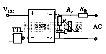
This document discusses the AC solid-state relay (AC-SSR) and presents its basic application circuit as illustrated in Figure (a). Additionally, it includes a TTL drive SSR circuit depicted in Figure (b), a CMOS driver circuit for the SSR shown...
This is a type of connection switch designed for incandescent lamps, known as a spider life extension switch. It has two main functions: First, it utilizes electroporation to enable semi-crossing buck starts and fully preheats the filament to transfer...
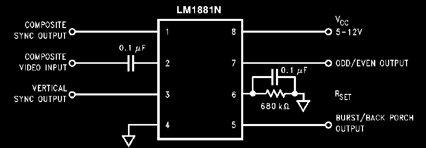
This is quite a nice chip, and has myriad uses, but we only need it to perform one function here. Since most game systems output the composite sync information along with the NTSC video output, and since most RGB...
Warning: include(partials/cookie-banner.php): Failed to open stream: Permission denied in /var/www/html/nextgr/view-circuit.php on line 713
Warning: include(): Failed opening 'partials/cookie-banner.php' for inclusion (include_path='.:/usr/share/php') in /var/www/html/nextgr/view-circuit.php on line 713