
28 LED Clock schematic
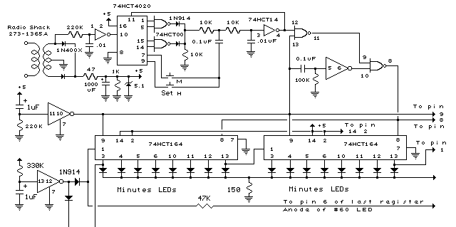
When power is applied, a single "1" bit is loaded into the first stage of both the minutes and hours registers. To accomplish this, a momentary low reset signal is sent to all the registers (at pin 9) and also a NAND gate to lock out any clock transitions at pin 8 of the minutes registers. At the same time, a high level is applied to the data input lines of both minutes and hours registers at pin 1. A single positive-going clock pulse (at pin 8) is generated at the end of the reset signal which loads a high level into the first stage of the minutes register. The rising edge of the first stage output at pin 3 advances the hours (at pin 8) and a single bit is also loaded into the hours register. Power should remain off for about 3 seconds or more before being re-applied to allow the filter and timing capacitors to discharge. A 1K bleeder resistor is used across the 1000uF filter capacitor to discharge it in about 3 seconds. The timing diagram illustrates the power-on sequence where T1 is the time power is applied and the beginning of the reset signal, T2 is the end of the reset signal, T3 is the clock signal to move a high level at pin 1 into the first register, T4 is the end of the data signal. The time delay from T2 to T3 is exaggerated in the drawing and is actually a very short time of just the propagation delay through the inverter and gate.
Two momentary push buttons can be used to set the correct time. The button labeled "M" will increment the minutes slowly and the one labeled "H" much faster so that the hours increment slowly. The hours should be set first, followed by minutes.
The circuit utilizes a total of 72 LEDs, with 60 dedicated to minute indication and 12 for hour indication. The architecture employs eight 74HCT164 shift registers for minute counting, where the output of each register cascades into the input of the next, effectively forming a 60-stage counter. The design ensures that only two registers are visibly connected to 16 LEDs for clarity, while the remaining registers follow the same connection schema. The feedback from the last register back to the first is critical for the continuous operation of the minute counting process.
The hour counting mechanism employs two 8-bit shift registers, functioning similarly to the minute section, but limited to 12 outputs corresponding to the hours of a clock. The interconnection of pin 9 across all shift registers allows for synchronized operation between the hour and minute counting sections.
For operation at 50 Hertz, the circuit requires a modification involving an additional 74HC30 IC to decode the requisite 7 bits from the counter. This adaptation is essential for maintaining accurate timekeeping at the specified frequency. The unused NAND gates in the 74HC00 are configured to ground, ensuring they do not interfere with the intended functionality.
The initialization sequence upon power application is crucial for ensuring proper clock operation. A reset signal is employed to clear the registers, followed by a clock pulse that loads the initial state into the first stage of both the minutes and hours registers. The timing elements, including a 1K bleeder resistor and a 1000uF capacitor, are designed to provide a clear discharge period of approximately 3 seconds, preventing erroneous clock states upon power restoration.
User interaction with the clock is facilitated through two momentary push buttons, allowing for manual adjustment of the time. The design prioritizes ease of use, ensuring that the hour setting is completed prior to minute adjustments for logical time setting.In the circuit below, 60 individual LEDs are used to indicate the minutes of a clock and 12 LEDs indicate hours. The power supply and time base circuitry is the same as described in the 28 LED clock circuit above. The minutes section of the clock is comprised of eight 74HCT164 shift registers cascaded so that a single bit can be recirculated through the 60 stages indicating the appropriate minute of the hour.
Only two of the minutes shift registers are shown connected to 16 LEDs. Pin 13 of each register connects to pin 1 of the next for 7 registers. Pin 6 of the 8th register should connect back to pin 1 of the first register using the 47K resistor. Pins 2,9,8, 14 and 7 of all 8 minutes registers (74HC164) should be connected in parallel (pin 8 to pin 8, pin 9 to pin 9, etc.). The hours section contains two 8 bit shift registers and works the same way as the minutes to display 1 of 12 hours.
Pin 9 of all 74HCT164s (hours and minutes) should be connected together. For 50 Hertz operation, the time base section of the circuit can be modified as shown in the lower drawing labeled "50 Hertz LED Clock Time Base". You will need an extra IC (74HC30) to do this since it requires decoding 7 bits of the counter instead of 4.
The two dual input NAND gates (1/2 74HC00) that are not used in the 50 Hertz modification should have their inputs connected to ground. When power is applied, a single "1" bit is loaded into the first stage of both the minutes and hours registers.
To accomplish this, a momentary low reset signal is sent to all the registers (at pin 9) and also a NAND gate to lock out any clock transitions at pin 8 of the minutes registers. At the same time, a high level is applied to the data input lines of both minutes and hours registers at pin 1.
A single positive going clock pulse (at pin 8) is generated at the end of the reset signal which loads a high level into the first stage of the minutes register. The rising edge of first stage output at pin 3 advances the hours (at pin 8) and a single bit is also loaded into the hours register.
Power should remain off for about 3 seconds or more before being re-applied to allow the filter and timing capacitors to discharge. A 1K bleeder resistor is used across the 1000uF filter capacitor to discharge it in about 3 seconds. The timing diagram illustrates the power-on sequence where T1 is the time power is applied and beginning of the reset signal, T2 is the end of the reset signal, T3 is the clock signal to move a high level at pin 1 into the first register, T4 is the end of the data signal.
The time delay from T2 to T3 is exaggerated in the drawing and is actually a very short time of just the propagation delay through the inverter and gate. Two momentary push buttons can be used to set the correct time. The button labeled "M" will increment the minutes slowly and the one labled "H" much faster so that the hours increment slowly.
The hours should be set first, followed by minutes. 🔗 External reference
Related Circuits
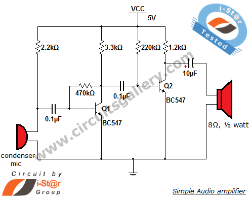
The output of the condenser microphone is coupled through a 0.1 µF coupling capacitor, which serves to eliminate DC components from the audio signal. Transistor Q1 is configured in a collector-to-base biasing mode, achieved with a 470kΩ resistor. This...
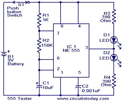
This schematic requires clarification. It is assumed that pin 2 is connected by a wire to pin 6, although this connection appears to be unclear. The circuit in question involves a schematic where pin 2 and pin 6 are interconnected....
This amplifier circuit utilizes three voltage levels: positive, negative, and ground, with a maximum voltage of approximately 55V DC. The circuit can accommodate several integrated circuits (ICs), including STK 030, 058, 075, 077, 078, 080, 082, 083, 084, and...
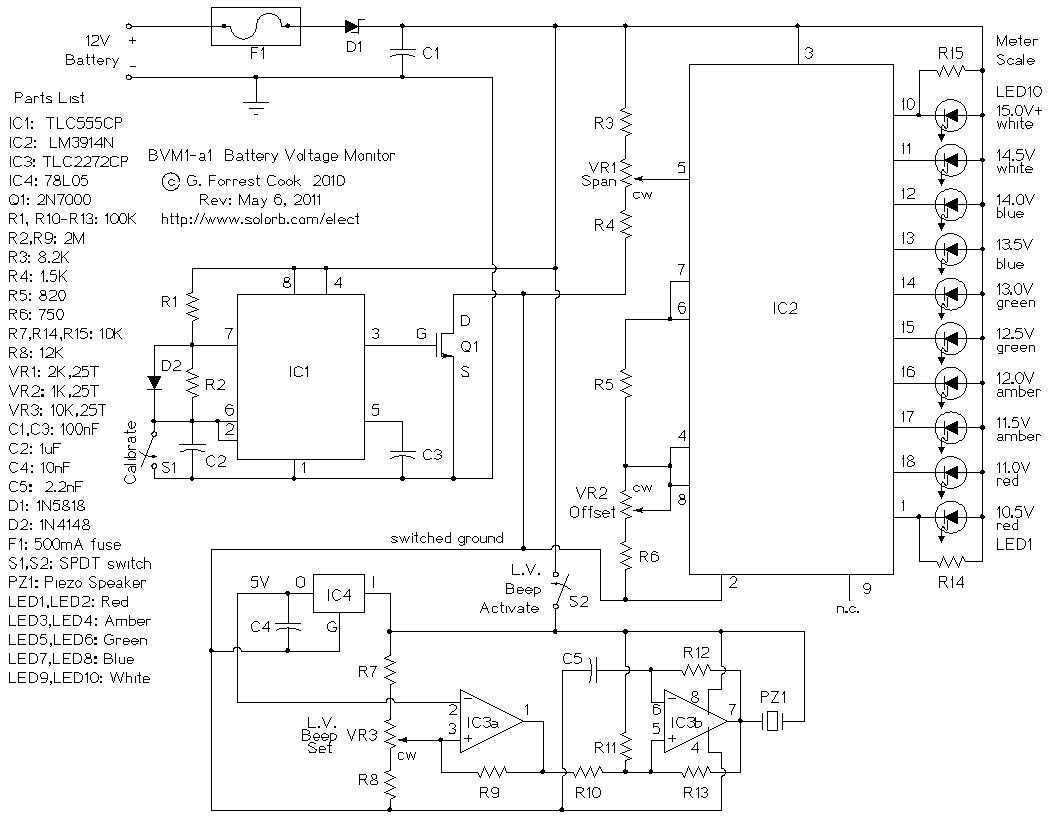
This is a low power voltmeter circuit that can be used with alternative energy systems that run on 12 and 24 volt batteries. The voltmeter is an expanded scale type that indicates small voltage steps over the 10 to...
This circuit converts the analog signal from the reversed LED, which is in sensing mode, and amplified by the operational amplifier, into a digital (on/off) signal. The original complex design has been simplified. An alternative approach is discussed in...
Most mobile chargers lack current and voltage regulation as well as short-circuit protection. These chargers supply unregulated 6-12V DC for charging battery packs. Typical mobile phone battery packs are rated at 3.6V and 650mAh. To enhance battery longevity, it...