
2meter 144mhz amateur radio transceiver
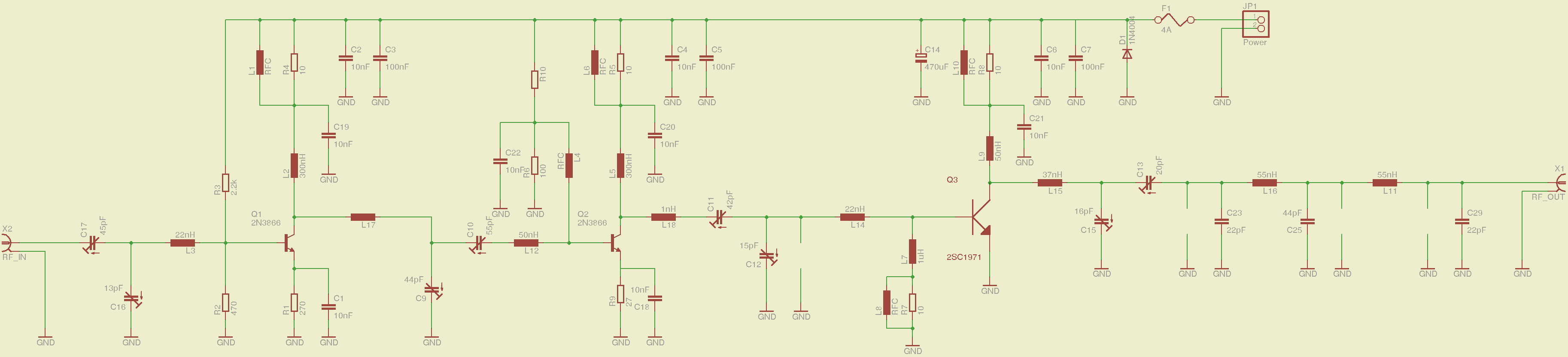
All schematics, PCB designs, and calculations for this project are available in the subdirectories of a public Git repository dedicated to RF circuits, particularly focusing on the MRF262 and MC3361 components. The VCO and PLL have two versions: the first utilizes a negative voltage pump generator to power operational amplifiers that bias the tuning varicap diode and mix digital/audio modulation, employing a MOSFET as the output driver. The second version includes a Wilkinson power splitter to yield two identical power outputs, one for the transmitter board and the other for the receiver board, eliminating the need for a negative voltage supply. Both versions utilize the LMX2305 digital PLL integrated circuit (IC), which requires a stable reference frequency provided by a crystal resonator; the internal division stages can be controlled through a three-wire interface directly from a microcontroller or desktop computer. The PLL IC does not contain an internal VCO, necessitating the design of a Clapp oscillator using a BFQ19 transistor, a small adjustable coil, and a BBY40 varicap tuning diode. This circuit block also includes a voltage regulator and several decoupling capacitors to ensure a clean output signal.
The PA consists of a three-stage bipolar transistor circuit and an output harmonic filtering bank, where the inter-stage matching circuits incorporate coils and tuning capacitors that must be adjusted for optimal efficiency and power gain. The 50-ohm input of this block connects to the VCO and PLL frequency synthesis block, while the 50-ohm output connects to the antenna. The microcontroller circuit block features a P16F84A operating at 4 MHz, with firmware programmed in assembly language. This firmware is responsible for programming the PLL and VCO circuit block with the transmission frequency when the push-to-talk (PTT) signal is activated, and the receiver frequency when receiving, as the receiver frequency is shifted by the first stage intermediate frequency (I.F.), which is 10.7 MHz in this case. A MAX236 is used for interfacing with a computer through the serial port; this IC was chosen because the RTS serial port pin activates the PTT signal. Users can select the operating channel frequency via desktop computer software or using two up/down channel buttons. The microcontroller also controls a RX/TX MOSFET pair to manage the antenna relay and other requirements within the transceiver.
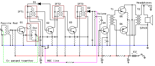
The transceiver includes three receiving blocks: the first is the LNA, the second reduces the VHF signal to the first 10.7 MHz I.F., and the third operates at a 455 kHz I.F. and includes a discriminator circuit for frequency modulation (FM) or frequency-shift keying (FSK) demodulation. Each block is equipped with filtering resonators surrounded by coil-transformer-capacitor impedance matching circuits, requiring minimal adjustments. The 10.7 MHz stage employs an NE602 IC, which contains a VCO and balanced mixer; the VCO is not utilized since the PLL and VCO block described earlier generates the necessary RX frequency. The 455 kHz stage uses a low-power narrowband MC3361 IC, which integrates a mixer, limiter amplifier, demodulator, and output signal amplifier. The output signal directly drives the FSK modem, with the software-based sound modem operating AX.25 in the 2-meter ham radio VHF band.A 2m ham radio transceiver that includes all the necessary circuitry, in particular the voltage-controlled oscillator ( VCO ) + phase-locked loop ( PLL ) for frequency synthesis, low noise amplifier ( LNA ) for the receiver front-end, power amplifer (PA) for the radio frequency ( RF ) output stage and PIC based micro-controller ( PIC ) with serial interface to computer desktop. All the schematics, pcb and calculations for this project can be found within the subdirectories of my public git repo dedicated to RF circuits, in particular mrf262 and mc3361. The VCO+PLL has two versions, the first one uses a negative voltage pump generator to supply power to the operational amplifiers responsible for biasing the tuning varicap diode and mixing in the digital/audio modulation and also uses a mosfet as the output driver.
The second version includes a Wilkinson power splitter to provide 2 identical power outputs, one for the transmitter board and the other for the receiver board and removes the need for the negative voltage supply. They both use the LMX2305 digital PLL I. C. , which needs a stable reference frequency, provided by a crystal resonator and the internal division stages can be controlled through a 3 wire interface directly from a micro-controller or desktop computer.
THE PLL I. C. doesn`t include an internal VCO, so a Clapp oscillator had to be designed around a BFQ19 transistor, a small adjustable coil and a BBY40 varicap tuning diode. This circuit block also includes a voltage regulator and a fair amount of decoupling capacitors to obtain a clean output signal.
The PA is a 3-stage bipolar transistor circuit and output harmonic filtering bank, where the inter-stage matching circuits include coils and tuning capacitors, which need to be adjusted for maximum efficiency and power gain. The 50 input of this block is connected to the VCO+PLL frequency synthesis block described above and the 50 output to the antenna.
The micro-controller circuit block contains a P16F84A running at 4MHz, with firmware programmed in the assembly language. The firmware is responsible for programming the PLL+VCO circuit block with the transmission frequency when the PTT signal is activated and the RX frequency when receiving since the RX frequency is shifted by the receiver first stage intermediate frequency ( I.
F. ), in this case 10. 7MHz. There`s also a MAX236 for interfacing with a computer through the serial port and this particular I. C. was selected since I use the RTS serial port pin to activate the PTT signal. A user can select the operating channel frequency through the desktop computer software or using two up/down channel buttons. The micro-controller also activates a RX/TX mosfet pair to be able to control the antenna relay and other needs in the rest of the transceiver.
The transceiver has 3 receiving blocks, the first one is the LNA, the second block is responsible from bringing down the VHF signal to the first 10. 7MHz I. F. and the third block with a 455kHz I. F. and the discriminator circuit for frequency modulation ( FM ) or frequency-shift keying ( FSK ) demodulation.
Each of these blocks have filtering resonators surrounded by coil-transformer-capacitor impedance matching circuits and require minimum adjustments. The 10. 7MHz stage uses a NE602 I. C. , which includes a VCO and balanced mixer; the VCO is not used since the PLL+VCO block described above provides the necessary RX frequency generation.
The 455kHz stage uses a lower power narrowband MC3361 I. C. which includes a mixer, limiter amplifier, demodulator and output signal amplifier. The output signal will then drive the FSK modem directly and in my case I use the software based soundmodem to operate AX. 25 in the 2m hamradio VHF band. 🔗 External reference
Related Circuits
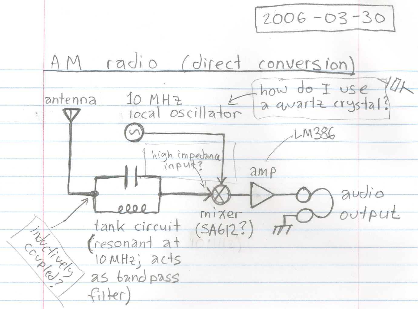
A basic design for a direct conversion AM radio receiver is being developed. "Direct conversion" refers to the technique of utilizing a mixer to shift the radio frequency signal down to baseband audio frequencies. There are uncertainties regarding the...
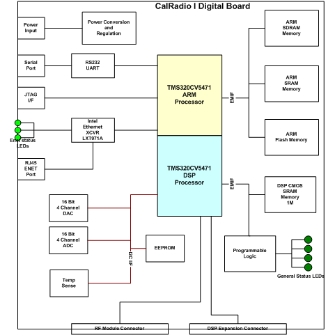
Cal-(IT)2 is developing several generations of general broad application radio/networking test platforms for wireless research and development. CalRadio I is the first generation. It provides a simple, low-cost platform for 802.11b development from the MAC layer and up. It...
Most surviving TR-1 radios no longer function. Many collectors prefer to maintain them in their original condition to preserve authenticity. However, there may come a time when one wishes to hear the radio play. Before proceeding with any modifications,...
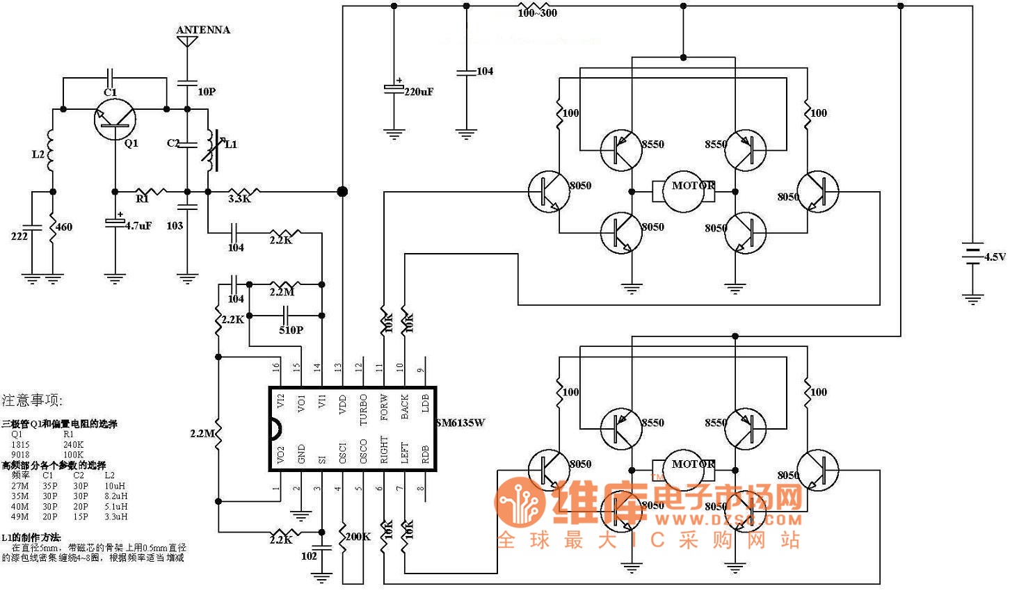
The diagram illustrates the principle circuit of a radio control car receiver. Important notes include the selection of transistor Q1, which is specified as either 1815 or 9018, along with the bias resistor R1, which has values of 240K...
An AM receiver depends on the original carrier signal (station frequency) being amplitude modulated, meaning the original amplitude (strength) varies at an audio rate. Figure 1 illustrates an unmodulated carrier signal as it might appear on an oscilloscope, showing...
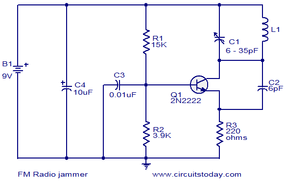
The circuit presented here can be used to jam FM radios in its vicinity. It consists of a classic single transistor oscillator operating in the VHF region. The working principle of the circuit is straightforward: powerful VHF oscillations from...