
3-D Depth Finding Imager with Digital Readout

The imager chip design for laser-scanned 3-D depth/range finding integrates two primary modules: the Pixel Array/Centroid Detection and the Analog-to-Digital Converter (ADC). The pixel array/centroid detection module is responsible for tracking the centroid of the laser beam as it scans the target object, while the ADC converts the analog signals generated by the centroid detection into a digital format for further processing.
The pixel array operates by scanning a laser beam across an object, where the vertical scanning is continuous and horizontal scanning is discrete. The reflected laser beam's interaction with the object's surface enables the imager to capture depth information through horizontal deflection. This deflection is critical for determining the spatial characteristics of the scanned object.
The system records the intensity of light incident on the imager as photocurrents across pixel columns. Instead of employing a basic winner-takes-all circuit that might yield only single pixel accuracy, the centroid detection system calculates the center of the intensity distribution, thereby achieving sub-pixel accuracy. This method necessitates fewer pixels, as only horizontal deflections are recorded.
To enhance the sensitivity and speed of the system, a single large photo column is utilized instead of multiple pixel outputs. This design choice maximizes the photosensitive area within a limited space, allowing for improved performance. The target specifications include achieving 30 fps with an image resolution of 128 x 128 pixels. Each photo column is designed to match the area of a single column of square photo pixels.
The choice of photodiodes over phototransistors is pivotal due to the faster response times of photodiodes and their lower capacitance characteristics, which are essential for maintaining high frame rates. The pixel support circuitry includes a cascoded inverting amplifier connected to an NMOS for feedback, which stabilizes the voltage on the N-Well, thereby optimizing the operational speed of the photodiode.
The design also allows for reduced spacing between adjacent N-Wells due to the clamping effect, which minimizes potential variations. This feature is critical in ensuring the accuracy of the centroid detection while mitigating issues related to photocurrent leakage. Overall, the design effectively combines advanced detection techniques with efficient circuitry to facilitate high-speed, high-accuracy 3-D imaging.The objective of the project is the design of an imager chip for laser-scanned 3-D depth/range finding. The project is divided into two modules: Pixel Array/Centroid Detection and Analog-to-Digital Conversion (ADC).
The pixel array/centroid detector tracks the centroid of the laser beam as its scans the object while the ADC converts the analog out put of the centroid into digital format. The conversion into digital ensures that the result is readily available for further processing in the digital domain. The pixel array/centroid detector is described first. The pixel and centroid system works in the following way. A laser is scanned across an object continuously in the vertical direction and discretely in the horizontal direction.
The laser beam reflects off the surface of the target. Because the imager observes the object from a different angle than that of the laser source, the surface depth is recorded as a horizontal deflection of the projected laser beam. The figure below illustrates the system overview. As the laser illuminates more than a single pixel, a distribution of the incident light intensity is recorded on the imager.
The discrete distribution is observed as photocurrents along columns of pixels of the imager. If we were to just use a winner-takes-all decision circuit to extract the horizontal deflection of the laser beam, we would be getting single pixel accuracy. By finding the center of this distribution we find our deflection value with sub-pixel accuracy. Only deflections in one axis are recorded and used. Therefore there is no need for a full N x N array of photo pixels. At the same time, the decision circuit will require that all the pixel output currents in a single column be summed together.
Rather than summing the pixel outputs, a single large photo column can be used. This has the added benefit of increasing the amount of photosensitive area that can be squeezed into the same space. The original goal was to achieve 30 fps at an accuracy of 128 x 128 pixels. Each photo column should have the same area as 1 column of square photo pixels. This large photosensitive area has a high capacitance. Therefore speed was the main design objective of the photo pixel support circuitry. Photodiodes were used rather than phototransistors for two reasons. The first is that phototransistors have a floating base and therefore react slower. Secondly photodiodes can be made from a junction of N-well and P-substrate, with significantly lower capacitance than a direct N-active to P-substrate junction.
At 128 x 128 pixel accuracy the photodiode has a capacitance of around 100 fF. This is large enough to hinder a 30 fps rate. Therefore the following pixel support circuitry was suggested. See schematic above. The output of the photodiode goes into a cascoded inverting amplifier which is then fed back to the output via an NMOS. This feedback circuit clamps the voltage on the N-Well. By keeping the voltage close to a constant, the photodiode does not need to charge and discharge the capacitance every time the photocurrent changes.
Therefore the desired speed is achieved, as shown in the simulation below. An interesting side benefit of clamping the voltages is the following. Normally a minimum of 18 lambda spacing is required between N-Wells at different potentials. But since the potential on the photodiode is being clamped any two adjacent photodiodes will be at very similar voltages. Therefore we can resort to the minimum N-Well spacing distance of 6 lambda. It should be mentioned that there is little side effect to photocurrent leakage from one photo pixel to the next, as this should not affect the centroid of the distribution to first order.
Below is the layout of the photopixel support circuitry (left) and the centroid (right). The next stage is the decision circuit. The centroid circuit can be seen in the schematic below [4]. The centroid circuit is a transconduc 🔗 External reference
Related Circuits
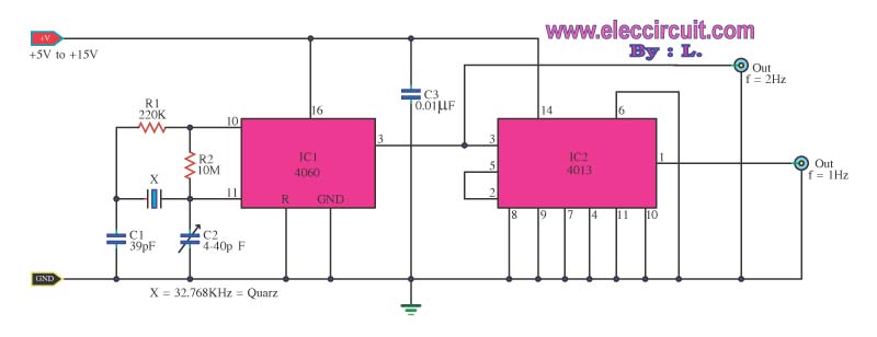
This is a standard digital clock circuit with a frequency of 1 Hz or 2 Hz. It can be utilized in a conventional clock circuit. The circuit comprises IC-4060 and IC-4013. The digital clock circuit operates by generating a precise...
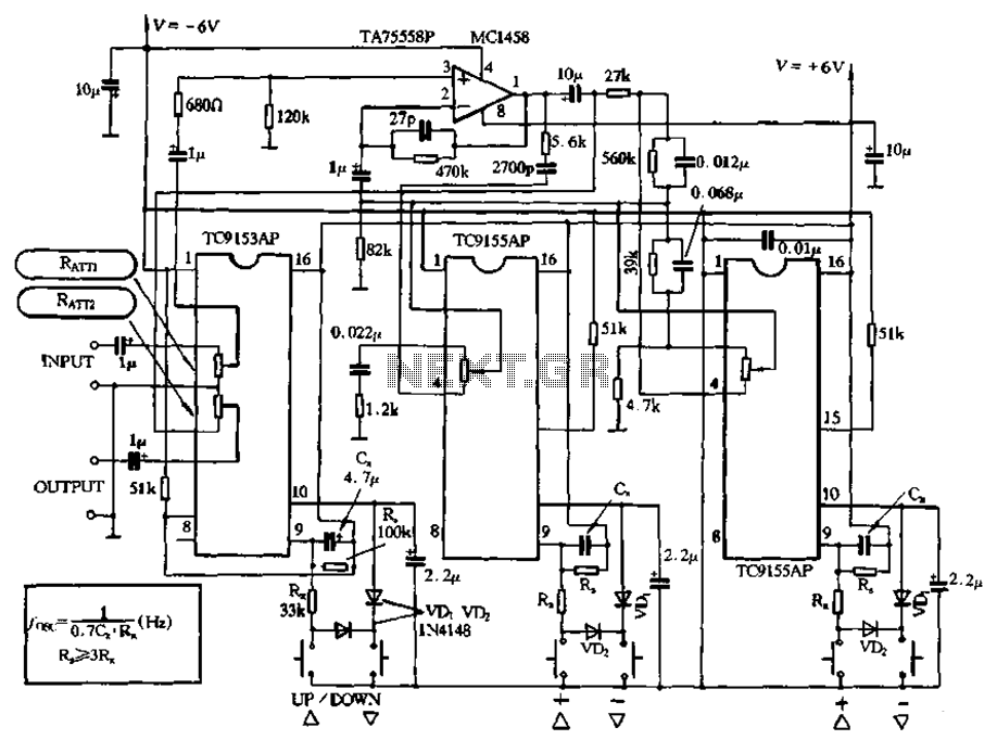
Figure 4-18 illustrates a volume potentiometer T (Xi 153AP) and a tone potentiometer T (155AP) that make up a volume and tone control circuit. This circuit includes Rx and Cx as clock oscillation elements, with values selectable based on...

An automatic inspection circuit designed for the simultaneous detection and control of multiple production equipment. This inspection circuit can perform sixteen regular inspections of production equipment. It consists of a pulse generator, multiple inspection circuits, and an automatic inspection...
This project will explain how I build my new wattmeter. This watt meter will be able to measure power from 300nW to 30W @ (0-500MHz). This wattmeter is based up on a dummy load of 50 ohm which can...
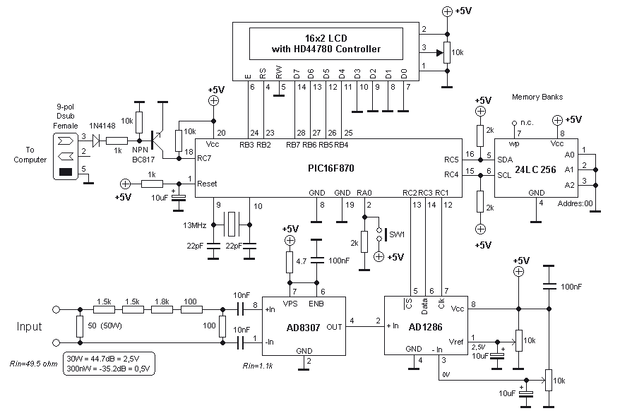
This project outlines the construction of a digital voltmeter utilizing a PIC microcontroller. A character LCD based on the HD44780 is employed to display the measured voltage. The PIC microcontroller used is the PIC16F688, which features 12 I/O pins,...
For beginners in microcontroller projects who are unsure where to start, this project serves as one of the simplest options available. It provides a clear understanding of programming a microcontroller. Often, one may glance at a watch and ponder,...