
300w power inverter circuit diagram
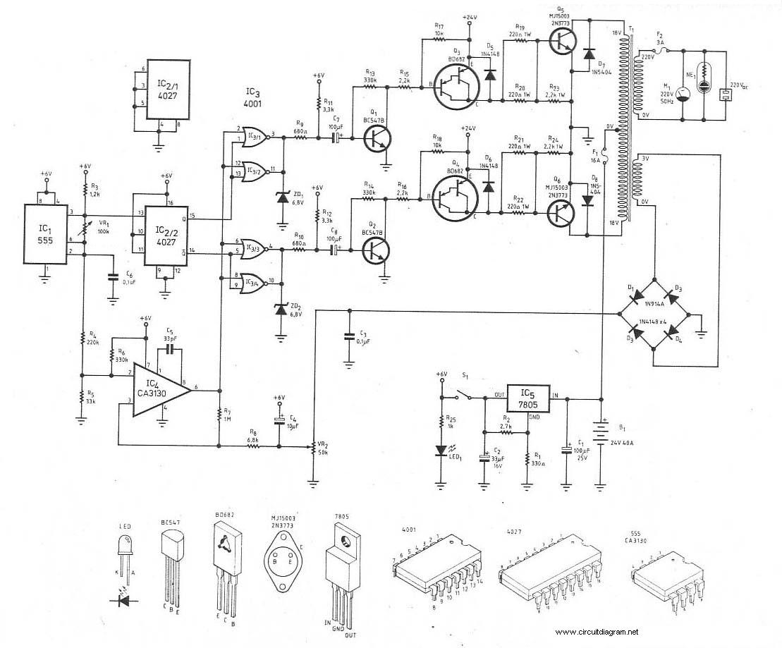
The 300W power inverter circuit is designed to efficiently convert a 24VDC input into a 220VAC output, making it suitable for various applications where AC power is required from a DC source. The use of the MJ15003 power transistor ensures reliable performance during the amplification stage. In scenarios where sourcing the MJ15003 is problematic, the 2N3773 serves as a viable alternative, maintaining the circuit's functionality.
The PCB layout design facilitates the assembly of the inverter, providing a clear and organized approach to component placement and soldering. This enhances the reliability and performance of the inverter once constructed. The inclusion of a 60W inverter circuit demonstrates the versatility of using 2N3055 transistors, which are known for their robustness in handling medium loads. Operating on a 12V battery with a minimum capacity of 15 Ah allows for efficient energy use, making it suitable for applications such as powering small appliances or devices.
The 500W inverter circuit expands the capability of these designs by utilizing multiple 2N3055 transistors to amplify the AC signal from the multivibrator. The multivibrator itself, constructed with transistors, generates the necessary frequency for the inverter operation. This configuration allows the inverter to handle larger loads, making it suitable for more demanding applications.
Lastly, the 100W inverter circuit showcases the use of the CD4047 IC, which is capable of generating a stable 50Hz sine wave signal essential for AC applications. The 2N3055 transistors in this circuit provide the necessary amplification to ensure that the output is sufficient for various devices. Overall, these inverter circuits exemplify practical and efficient designs for converting DC to AC power, utilizing readily available components for ease of assembly and application.This is the schematic diagram of 300W power inverter circuit. The inverter uses power transistor MJ15003 for final amplification. You may replace the MJ15003 with 2N3773 if you have difficulty to find MJ15003 transistor. The inverter will convert 24VDC to 220VAC voltage. Here the PCB layout design for 300W Power. This is a 60 Watts inverter circu it diagram which using a couple power transistor of 2N3055 for final amplification. Actually, the circuit is capable of driving medium loads of the order of 40 to 60 watts working with battery of 12V, 15 Ah or greater capacity. This inverter will convert. This is the scheme diagram of 500W power inverter circuit which build using 10 pieces of well-known NPN power transistor 2N3055 to amplify the AC signal produced by multivibrator.
The frequency generator / multivibrator is built based on transistors too. All of the components is easy to gathered from the. This is the schematic diagram of 300W power inverter circuit. The circuit use timer IC NE555 as to produce the wave / AC voltage signal. The signal the fed to the final amplifier to be amplified and to powered up the signal. There are many 2SD1047 transistor to amplify the. Here the schematic diagram of 100W Inverter Circuit which will convert 12VDC input to be 220VAC output. The circuit built based IC CD4047 to generate sine wave signal 50Hz and then the power transistor 2N3055 will boost the signal so that the signal have high power (high electric current).
Then. We aim to transmit more information by carrying articles. Please send us an E-mail to wanghuali@hqew. net within 15 days if we are involved in the problems of article content, copyright or other problems. We will delete it soon. 🔗 External reference
Related Circuits
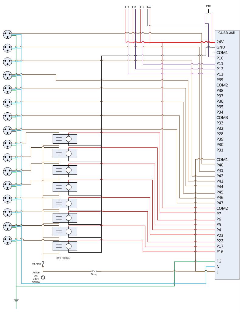
This is the circuit diagram for the Comfile CUSB-36R Programmed Christmas Lights. If it is difficult to read, please contact me via email at [email protected], and I will provide a more detailed schematic. The Comfile CUSB-36R can either drive...
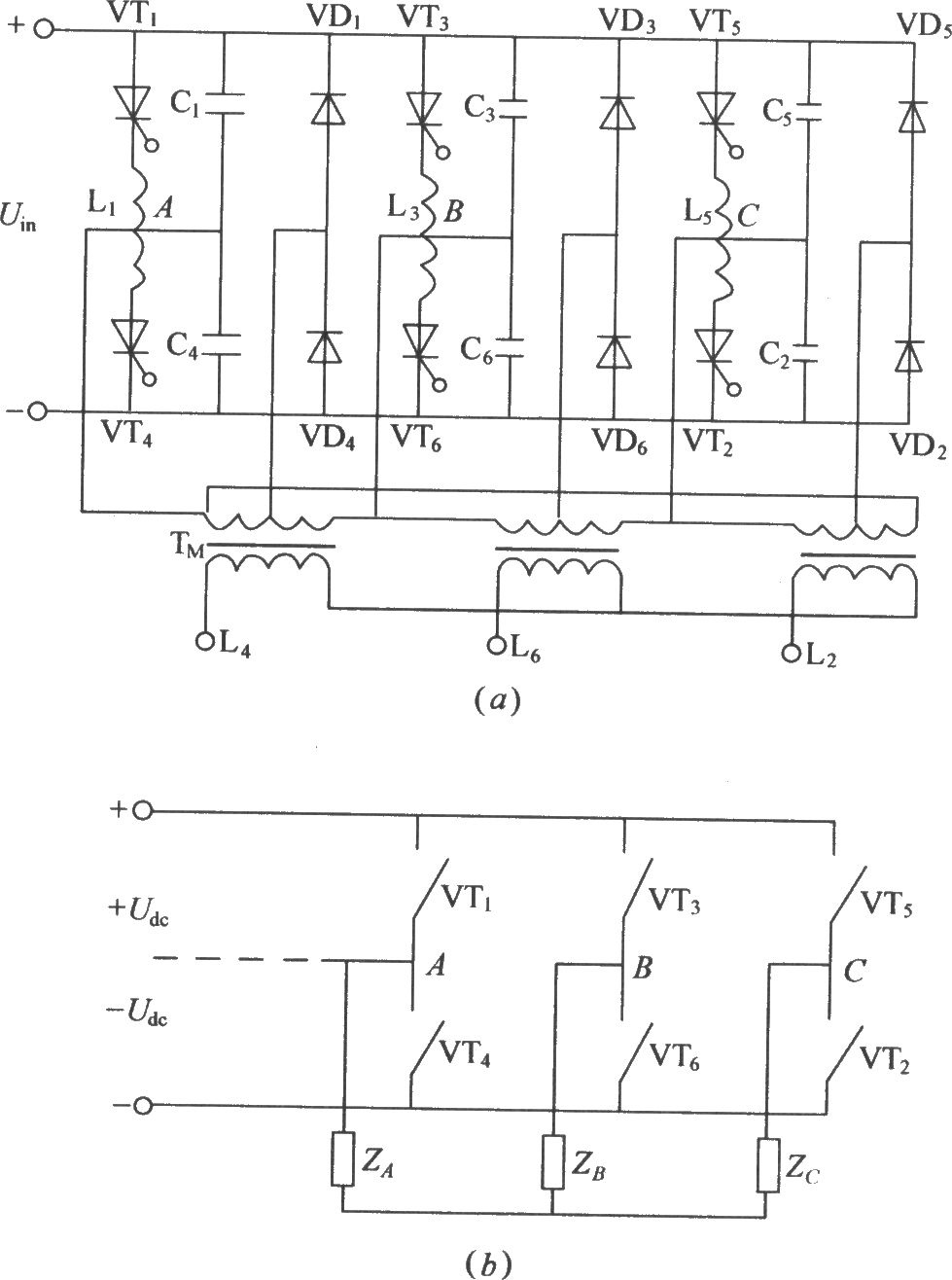
The figure illustrates a traditional three-phase bridge inverter circuit. Components VT1 to VT6 represent thyristors, while L1 to L6 are commutation reactors. Capacitors C1 to C6 serve as commutating capacitors, and the thyristor shut-off circuit is composed of two...
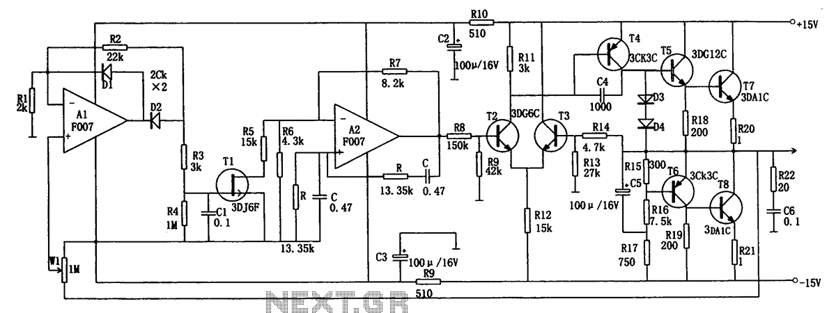
The low-frequency signal generating circuit demonstrates excellent performance characterized by stable operation, high output power, and minimal waveform distortion. It serves as an ideal source for low-frequency measurement signals. The circuit includes an operational amplifier (A) with a feedback...
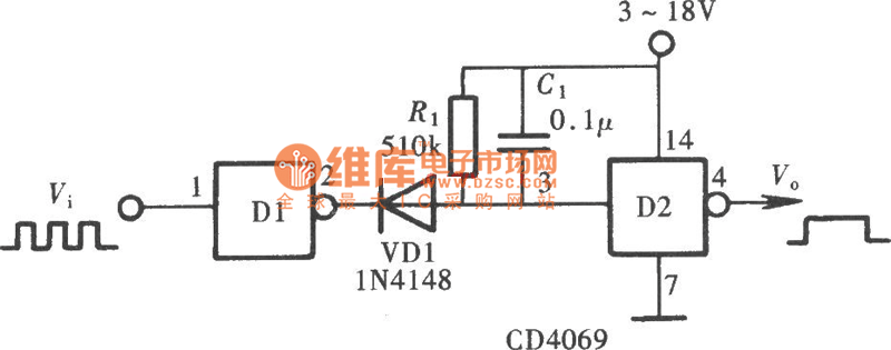
The Pulse Demodulator, as illustrated in the accompanying image, consists of a CMOS Hex Inverter. This circuit is capable of performing envelope detection on amplitude pulses. The Pulse Demodulator utilizing a CMOS Hex Inverter is designed to extract the envelope...
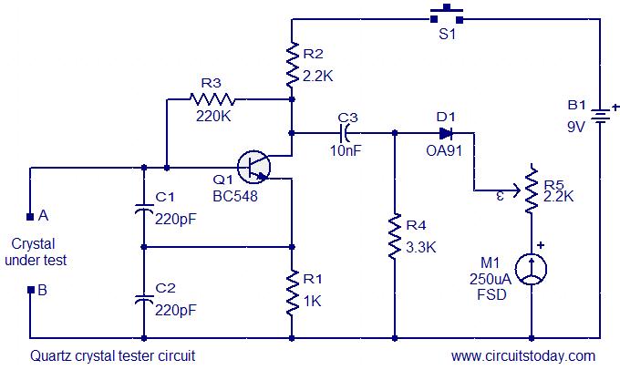
This is a straightforward and cost-effective circuit designed for testing quartz crystals. A Colpitts oscillator is employed using transistor T1. When the crystal is connected between terminals A and B, the circuit generates high-frequency oscillations. These oscillations will only...
A real-size printout of the PCB is created to verify the dimensions of all components against it. If a component is too large or small to fit its PCB pads, adjustments to the PCB layout can be made, or...
Warning: include(partials/cookie-banner.php): Failed to open stream: Permission denied in /var/www/html/nextgr/view-circuit.php on line 713
Warning: include(): Failed opening 'partials/cookie-banner.php' for inclusion (include_path='.:/usr/share/php') in /var/www/html/nextgr/view-circuit.php on line 713