
3V Supply Splitter
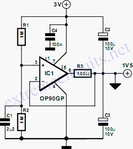
The described circuit serves a crucial role in enabling modern electronic devices to operate efficiently from a single supply voltage. The potential divider formed by resistors R1 and R2 accurately bisects the 3V supply, producing a stable 1.5V virtual ground. This virtual ground is essential for providing a reference point for other circuit components, ensuring consistent performance.
The use of an op amp as a buffer is a strategic choice, allowing for high input impedance and low output impedance, which is vital for maintaining signal integrity. The op amp's output is decoupled by capacitors C2 and C3, which not only stabilize the voltage but also filter out high-frequency noise, thus preserving the quality of the virtual ground.
Feedback from the junction of C2, C3, and R3 to the inverting input of the op amp forms a negative feedback loop, which enhances the linearity and stability of the output voltage. Resistor R3 plays a significant role in ensuring that the circuit can handle variations in load without affecting the output voltage, maintaining performance even when the load changes.
The ability of the circuit to regulate ±2mA is indicative of its utility in various applications where small current levels are needed. The low overall current drain of 13 µA, primarily due to the high resistance values of R1 and R2, makes this circuit suitable for battery-operated devices, prolonging battery life and ensuring efficiency.
Moreover, the op amp's capability to function at a minimum voltage of 1.6V allows the circuit to remain operational even as the supply voltage drops, a common scenario in battery-powered applications. This feature is particularly advantageous in ensuring continuous operation until the battery is fully depleted, providing reliability in critical applications.
In summary, this circuit design exemplifies an effective approach to creating a virtual ground in modern electronic systems, balancing performance, efficiency, and reliability.Many modern circuits tend to work from a single supply voltage of 3V. But often they need a virtual earth at half the supply voltage for efficient operation. The splitter shown in the diagram bisects the supply voltage with a high-resistance potential divider, R1-R2, and buffers the resulting 1. 5 V line with an op amp. Since the op amp used is not a fast type, the output is decoupled by capacitive divider C2-C3. This ensures that the impedance of the virtual earth point remains low over a wide frequency band. Because the potential at the junction C2-C3-R3 is fed back to the inverting input of IC1, the circuit becomes a standard voltage follower. Resistor R3 ensures that the regulation remains stable. The circuit can regulate ±2mA without any difficulties. Because of the low current drawn by IC1, and the high resistance of R1 and R2, the overall current drain is low.
In the absence of a load, it was 13 µA in the prototype, of which 1. 5 µA flows through R1-R2. Finally, since IC1 can operate from a voltage as low as 1. 6V, the splitter will remain fully operational when the battery nears the end of its charge or life. 🔗 External reference
Related Circuits
This supply can function as a battery eliminator for various devices, such as tape recorders, small radios, clocks, and more. A resistance is selected to provide a predetermined output voltage. In this circuit, various commonly used supply voltages produced...

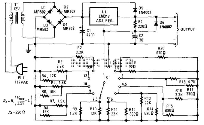
The circuit presented is an economical smooth variable power supply that provides an output range of 0V to 24V. It incorporates all necessary controls and short circuit protection while maintaining acceptable regulation and a ripple-free output, utilizing a minimal...
This is a low-cost protection circuit designed to safeguard electrically operated home appliances, such as TVs, DVD players, refrigerators, and other devices, during sudden power outages and the subsequent restoration of mains supply. Appliances like refrigerators and air conditioners...
This 8V DC power supply is designed for use with high-end electronic equipment. It includes full over-voltage protection to safeguard against regulator failure, whether in the supply itself or in the connected device. The circuit employs a standard full-wave...
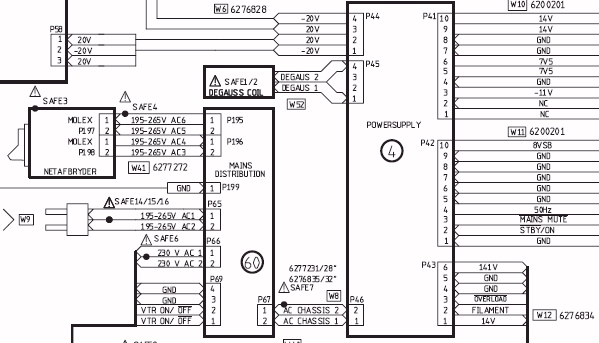
The AVANT employs a Switched Mode Power Supply (SMPS), which is centered around a 32 kHz ramp oscillator. This oscillator ceases operation if the overload protection circuit identifies an overload condition. When the oscillator is inactive, the 8-volt standby...
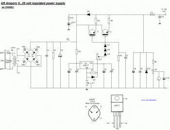
This is a simple power supply that provides a reliable and clear regulated output voltage ranging from 0 to 28 volts with a maximum current of 6 to 8 amperes. Utilizing two 2N3055 transistors allows for doubling the output...