
4017 gate sequencer

The 4017 decade counter is a versatile IC commonly used in sequencing applications. When cascading multiple 4017s, it is essential to ensure that the reset and clock signals are properly managed to avoid erratic behavior. The cascading allows for an expansion of the number of outputs, enabling more complex sequences. The use of AND gates in conjunction with the 4017s allows for more precise control over the sequencing, as the gates can be configured to enable or disable steps based on specific conditions.
In a typical application, the clock signal is fed into the AND gates, which are configured to gate the clock pulses to the respective 4017 inputs. This gating can be tailored to create specific patterns or sequences, enhancing the functionality of the sequencer. The output pins from the 4017s can drive various loads, such as LEDs or relays, depending on the design requirements. The use of a 555 timer for PWM control provides additional flexibility, allowing for modulation of the output signals.
To achieve reliable performance, careful attention must be paid to the power supply levels and the timing components used in the circuit. Resistor and capacitor values should be selected based on the desired frequency and duty cycle of the output signals. Additionally, ensuring that the circuit is breadboarded correctly and that all connections are secure will help prevent issues such as skipping steps or freezing.
In summary, the design of a dual 4017 sequencer with AND gates offers a robust solution for creating extended sequences. By addressing potential issues related to high-frequency operation and ensuring proper configuration of components, a stable and functional sequencer can be realized.The cool thing about the 4017 is that you can add other 4017s and make the sequence longer (of course with more discrete parts): I saw the schematic youG ‚¬ re talking about. Oddly, this was one of the only 4017 cascading schematics I could find. I found that it was REALLY temperamental and more of a headache than it was worth at the time. Fir st off I had to change some of the resistor values before it even worked. Then it was only looping ONE 4017 sequence at 12 volts. At 5 volts it worked better, but would skip some steps. It was probably an error on my end, but I bread boarded it twice and it acted the same both times. My original thought was that I would combine 2 4017s together to make a 16 step sequence. That way I could get 8 distinct output pulses. If youG ‚¬ ve tried making a gate sequencer with the 4017 you probably know that you need to use every other step as an G ‚¬ OFFG ‚¬ step. So in an 8 step sequence, you only get 4 G ‚¬ ONG ‚¬ pulses. Anyway, as I mentioned, the circuit you mentioned above was acting real bonkersG ‚¬ so I investigated some other options, hence the AND gate output stage.
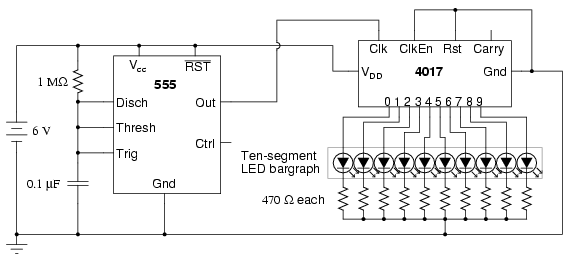
it wight work to use a 555 as PWM. i have never done this myself. but it has a trigger input, and it can do PWM. so this might be a solution. although im totally unsure about it. look here hey, i don`t know anything about those AND gates, but i do know that if you use pin 7 to ground your 4017 ²s leds instead of the main ground you can get 10 relay trigger signals. Thats how ive done it in the past. I guess you don`t get the gate time control but the schematic is quite a bit easier. hey, i`ve been planning to build a sequencer for a while, and i think i`ve cracked the dual 4017 nut, allowing for 16 steps.
I thought i`d post a rough outline as i`ve gotten alot of inspiration from your work and website and i thought i`d try to give something back. the clock source is connected to one input of two AND gates (lets say gate-a and gate-b. I used a 4081 but any AND gate ic will do. The output of gate-a is connected to pin 14 of 4017-a and the output of gate-b is connected to pin 14 of 4017-b.
The second input of gate-a is connected to pin 3 of 4017-b, and the second input of gate-b is connected to pin 9 of 4017-a. Both of the 4017 have pins 15 and 11 connected together. Thats it. Pins 3-6 of 4017-a are the first 8 steps of the sequence and pins 2-9 of 4017-b are the last 8. This rest of the circuit is the same as your step sequencer, using another 4018 AND gate to cut the steps and a 4016 as a gate (i`ve used 9v and changed the resistor values but this should make no difference).
I have found one frustratingly glitch with the circuit. It locks at both step one and nine when it`s clock at very high frequencies. I`ve found that disconnecting pin 11 from 15 on 4016-b and connecting pin 11 to 12 breaks it out of this freeze. I think capping the frequency below the freeze point would be the best option, and not really a hassle as it is a very high frequency.
Other than that the circuit seems pretty stable, and better than anything else i`ve come up with as the number of steps can be changed easily by moving the reset pin connection on 4017-b. 🔗 External reference
Related Circuits
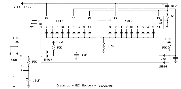
The question sometimes comes up of how to cascade 4017 decade counters for more than 10 sequential stages. The LED sequencer below shows a possible solution using a few extra parts. When power is applied, the 15K resistor and...
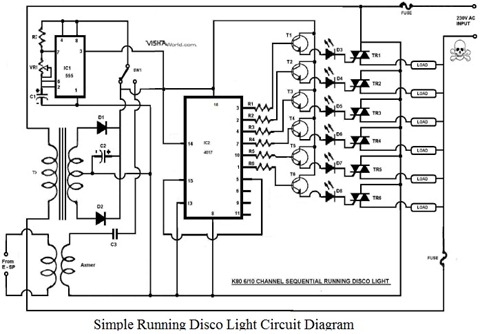
This article explains how to design a minimal Running Disco Light Circuit Diagram using the IC 4017. The IC 4017 is a 16-pin dual in-line package integrated circuit that includes a 10-stage decade counter. The design operates on 230V...
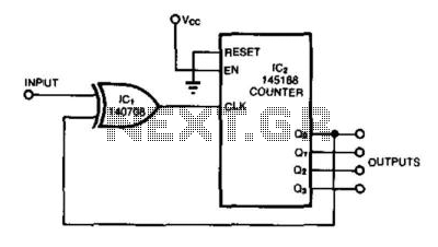
Inverting the negative-going input transitions allows the counter to count both positive and negative-going edges. The XOR gate transforms the input signal into a series of short pulses whose width is equal to the sum of the counter and...
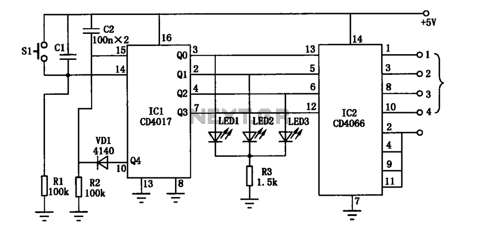
The electronic circuit diagram consists of the CD4017 and CD4066 components configured as a switch circuit. The CD4017 is a decade counter integrated circuit (IC) that can drive up to ten outputs, sequentially activating them based on clock pulses. It...
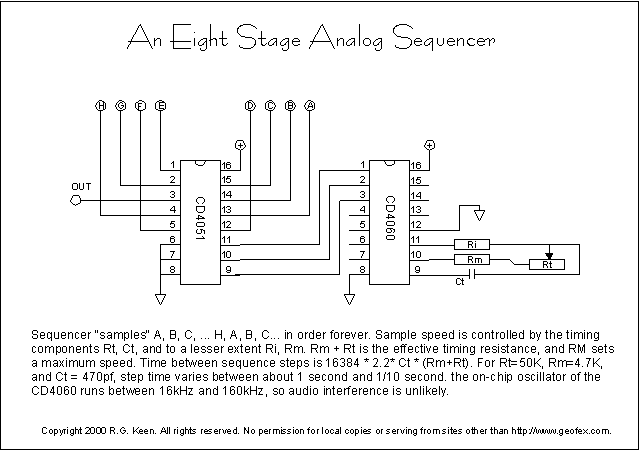
The CD4060 is a CMOS 14-stage binary counter with an internal oscillator on chip. The oscillator is controlled by the resistors and capacitor tied to the timing pins, 9-11. This oscillator runs the binary counter, and the various outputs...
The model 4017 integrated circuit is a CMOS counter with ten output terminals. At any given time, one of these ten terminals will be in a "high" state, while all others remain "low," resulting in a "one-of-ten" output sequence....