
50mW Class-A Headphone Amplifier
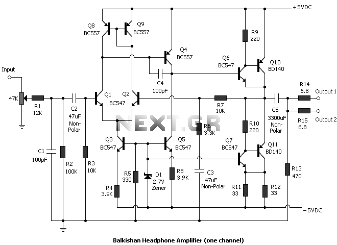
My headphone amplifier is a conventional VFB type employing commonly available parts. Let's consider a typical VFB setup using BJT transistors. We have a differential pair input stage, a voltage gain stage, an output (current gain) stage and a -ve feedback network. For the explanation, I will not include the current gain stage since it has no role to play as far as the voltage gain is concerned. The voltage gain stage is a CE stage with a constant current source (CCS) for the collector resistor and theoretically has an infinite voltage gain as per the above formula (the output impedance of a true CCS is infinite). Also note that the presence of a CCS minimises the variation in gain due to hie, which becomes extremely small and can be neglected, and also makes the use of an emitter resistor unnecessary. The output stage is comprised of the compound emitter follower Q6/Q10 and the compound current source Q7/Q11 which biases the emitter follower at about 124mA, which is about 10% higher than the peak output current (110mA, measured at the transistor side of C5). Q7/Q11 form the CCS along with D1 and R11/R12. This amp does not use any push-pull arrangement for the output stage.
CCS operation: The voltage across R11/R12 is the zener diode voltage less the Vbe drop of Q7 (about 2V). This means that if the diode voltage is constant, the current through R11/R12 will be constant => current in the emitter terminal of compound pair Q7/Q11 is constant => since, Ic = Ie (neglecting base current) the current in the load (Q6/Q10) connected to the CCS will be constant. R5 provides the diode current. Note that in the prototype, I have used LEDs in place of zeners. This is fine, except that a slight reduction in the output stage bias current will occur and the LEDs must be connected in a direction opposite to that of the zener (pointing downwards instead of upwards, in the schematic).
The closed-loop gain (excluding the input attenuator formed by R1, R2 and R3) is 1 + R7 / R6, as it is used as in the non-inverting mode. Here, R6 and R7 set the gain at 12dB. The gain is measured as the ratio of voltages (RMS) at the collector of Q10 and the base of Q1. R1 and R3 form an attenuator to decrease the input sensitivity of the amplifier to about 850mV for an output power of 50mW. To increase the sensitivity, R1 can be reduced. Changing the gain of the amplifier is possible by changing the feedback resistors R6 and R7. In the case of my amp, the feedback resistors have already fixed the gain to a value higher than needed and the input signal is attenuated to compensate for this. So to change the overall gain either the attenuator resistors can be changed or the -ve feedback resistors can be changed. If the attenuator is changed then the input caps must also be changed to maintain the lower and higher -3dB frequency points. All electrolytics must preferably be bypassed with 100nF capacitors (not shown in the schematic). The 100nF caps are ceramic types, but film caps may be used (it is doubtful if any audible improvement will occur). C5 is used to prevent any DC from reaching the phones in the event of output device failure. Although a failure is very improbable, it has been included as a fail-safe, and can be omitted if a small amount of DC offset is acceptable. With C5 in place, the lower -3dB frequency becomes about 3 Hz with both A and B phones connected (1.8 Hz with either A or B). If C5 is not used, then C2 may be chosen to get a lower -3dB frequency of about 3 to 5 Hz. The amplifier may be used with headphones having an impedance of 32 Ohms or higher.
The transistors need not be very critically matched. For the power devices, the range of hfes allowable is 50 to the maximum available for BDxxx devices and the matching has to be done to ensure that hfes are within 20% to 30% of each other. As for the BCxxx devices the same above rules apply. The minimum hfe being 100. It may be noted that the output stage is a compound pair and as such, the combined hfe (of Q6/Q10 and Q7/Q11) is very high, making the absolute values and matching less critical.
The headphone amplifier is designed as a voltage feedback (VFB) Class A amplifier to drive two sets of headphones from a computer sound card. The circuit features a differential input stage followed by a common emitter (CE) voltage gain stage and a compound emitter follower output stage. The differential input stage is critical for minimizing common-mode noise and improving sound quality. The gain of the amplifier is primarily determined by the feedback resistors R6 and R7, allowing for adjustments in gain while maintaining stability.
The constant current source (CCS) in the voltage gain stage enhances linearity and reduces distortion, as it effectively decouples the gain from variations in transistor parameters. The output stage is designed to handle the required current levels for headphone operation, ensuring that the amplifier can deliver up to 50mW of power into loads with impedances of 32 Ohms or higher.
The inclusion of capacitors such as C5 serves as a DC blocking mechanism to protect the headphones from potential DC offsets, while the careful selection of resistor values allows for tailored input sensitivity and frequency response. Overall, this amplifier design is optimized for performance, simplicity, and reliability, making it suitable for various headphone applications.This amplifier was born out of a need to use two sets headphones with my computer's sound-card. The design presented here is a 50mW power amplifier meant for phones with impedances of 32 Ohms and greater. I chose this class A topology, because it offers very good distortion figures without a lot of complexity.
A simple common emitter amplifier, for example, is not very linear and the overall gain is very much device dependent. In the case of my amp, it uses a voltage feedback (VFB) topology, and the gain is dependent only on the ratio of 2 resistors.
Plus, the amp has very good power supply and common mode rejection on account of the differential input pair and the current source used to bias it. With a simple common emitter amplifier, the gain is given by the formula (assuming hfe >> 1) Av = hfe * Rc / [(hfe * Re + hie)]. hfe is the transistor current gain and hie is its base-to-emitter resistance. Rc is the collector (or load) resistor which biases the transistor and Re is the emitter resistor which provides bias stabilisation and local -ve feedback.
hie is device dependent and highly non-linear. It varies with the collector (or emitter) current and causes the gain to vary with the collector current, resulting in distortion. If Re is large enough to make hie negligible, then Rc will also need to be large and the amplifier won't be able to source/sink current into low-impedance loads.
My headphone amplifier is a conventional VFB type employing commonly available parts. Let's consider a typical VFB setup using BJT transistors. We have a differential pair input stage, a voltage gain stage, an output (current gain) stage and a -ve feedback network. For the explanation, I will not include the current gain stage since it has no role to play as far as the voltage gain is concerned.
The voltage gain stage is a CE stage with a constant current source (CCS) for the collector resistor and theoretically has an infinite voltage gain as per the above formula (the output impedance of a true CCS is infinite). Also note that the presence of a CCS minimises the variation in gain due to hie, which becomes extremely small and can be neglected, and also makes the use of an emitter resistor unnecessary.
The output stage is comprised of the compound emitter follower Q6/Q10 and the compound current source Q7/Q11 which biases the emitter follower at about 124mA, which is about 10% higher than the peak output current (110mA, measured at the transistor side of C5). Q7/Q11 form the CCS along with D1 and R11/R12. This amp does not use any push-pull arrangement for the output stage. CCS operation: The voltage accross R11/R12 is the zener diode voltage less the Vbe drop of Q7 (about 2V).
This means that if the diode voltage is constant, the current thru' R11/R12 will be constant => current in the emitter terminal of compound pair Q7/Q11 is constant => since, Ic = Ie (neglecting base current) the current in the load (Q6/Q10) connected to the CCS will be constant. R5 provides the diode current. Note that in the prototype, I have used LEDs in place of zeners. This is fine, except that a slight reduction in the o/p stage bias current will occur and the LEDs must be connected in a direction opposite to that of the zener (pointing downwards instead of upwards, in the schematic).
The closed-loop gain (excluding the input attenuator formed by R1, R2 and R3) is 1 + R7 / R6, as it is used as in the non-inverting mode. Here, R6 and R7 set the gain at 12dB. The gain is measured as the ratio of voltages (RMS) at the collector of Q10 and the base of Q1. R1 and R3 form an attenuator to decrease the input sensitivity of the amplifier to about 850mV for an output power of 50mW.
To increase the sensitivity, R1 can be reduced. Changing the gain of the amplifier is possible by changing the feedback resistors R6 and R7. In the case of my amp, the feedback resistors have already fixed the gain to a value higher than needed and the input signal is attenuated to compensate for this. So to change the overall gain either the attenuator resistors can be changed or the -ve feedback resistors can be changed.
If the attenuator is changed then the input caps must also be changed to maintain the lower and higher -3db frequency points. All electrolytics must preferably be bypassed with 100nF capacitors (not shown in the schematic). The 100nF caps are ceramic types, but film caps may be used (I really doubt if it'll have any audible improvement though).
C5 is used to prevent any DC from reaching the phones in the event of o/p device failure. Although a failure is very improbable, I have included it as a fail-safe, and can be omitted if a small amount of DC offset is acceptable. With C5 in place, the lower -3dB frequency becomes about 3 Hz with both A and B phones connected (1.8 Hz with either A or B).
If C5 if not used, then C2 may be chosen to get a lower -3dB frequency of about 3 to 5 Hz. The amplifier may be used with headphones having an impedance of 32 Ohms or higher. The transistors need not be very critically matched. For the power devices, the range of hfes allowable is 50 to the maximum available for BDxxx devices and the matching has to be done to ensure that hfes are within 20% to 30% of each other. As for the BCxxx devices the same above rules apply. The minimum hfe being 100. It may be noted that the output stage is a compound pair and as such, the combined hfe (of Q6/Q10 and Q7/Q11) is very high, making the absolute values and matching less critical.
🔗 External reference
Related Circuits
Headphone Amplifier or Pre-Amplifier Output Stage. This 1-watt amplifier is ideally suited for use as a driver for low-impedance headphones. The headphone amplifier circuit is designed to provide an amplified audio signal to drive low-impedance headphones effectively. Operating at a...

The 25-watt audio amplifier circuit is powered by a tube circuit. The tube transistor (TR) will amplify the input to approximately 20 watts, while a dual transformer can increase the output to 40 watts. A wide voltage range of...
The circuit design aims to create a preamplifier for television systems that operates within the UHF frequency range of 450 MHz to 800 MHz. The preamplifier circuit is essential for enhancing weak television signals before they are processed by the...
This 900 MHz amplifier circuit is constructed using the BFG480W transistor, which exhibits excellent linearity performance. As a result, the BFG480W is highly suitable for low-noise amplifiers (LNAs) that require high linearity. The 900 MHz amplifier circuit utilizing the BFG480W...
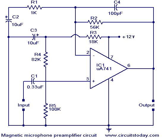
A preamplifier for magnetic pickups of record players is presented. The uA 741 is utilized as an AC-coupled non-inverting amplifier operating on a single supply. The amplifier gain is determined by the feedback components, where C2 manages the low-frequency...
TDA2004 Car Battery 12W Stereo Amplifier Circuit. Its main features are low distortion, low noise, and high reliability of the chip. The TDA2004 is a highly integrated audio amplifier designed specifically for automotive applications. This circuit is capable of delivering...