
50W class AB amplifier
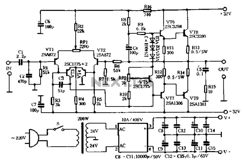
The described pure Class AB output stage amplifier circuit is designed to provide a balance between performance and simplicity, making it an attractive option for enthusiasts and professionals alike. The differential amplifier formed by transistors VTI and VT4 allows for effective signal amplification while minimizing distortion. The choice of components, particularly the power output transistors VT6 and VT7, is crucial for achieving the desired output characteristics, including linearity and thermal stability.
To further elaborate on the circuit's operation, the biasing network involving diodes VD1, VD3, and VD5 plays a vital role in ensuring that the output transistors operate in their optimal range, thus enhancing the overall fidelity of the amplifier. The resistors R6 and R7 not only control the gain but also help in setting the input impedance of the amplifier, which is essential for matching with various audio sources.
The adjustment process outlined is critical for fine-tuning the amplifier's performance. Setting the midpoint potential to 0V with RP1 ensures that the amplifier operates in a balanced state, preventing crossover distortion. The adjustment of RP2 to achieve a voltage of approximately 0.1V across R13 is indicative of the quiescent current flowing through the output stage, which is key to maintaining the Class AB operation without significant thermal runaway.
Overall, this amplifier circuit represents a practical solution for those looking to build a high-quality audio amplifier without delving into overly complicated designs. The straightforward nature of the circuit, combined with the clear adjustment procedures, makes it accessible for both novice and experienced builders.Fans are hoping to make a high-quality amplifier, but the most outstanding publications published on the circuit, they often too complex and difficult to start 6 This article d escribes a pure class AB output stage amplifier circuit, the circuit is simple, sound quality is satisfactory, Hing interested persons may wish to try the heart of the circuit shown in Figure 4-3. VTI ~ VT4 composed of one, two differential amplifier, VT6 ~ VT7 constitute power output tube, VT8VT9 to promote o VDl --VD3VT5 circuit providing a bias to VT6 ~ VT9.
Gain of the circuit by the R6, R7 control about 30 times. The entire circuit is simple and clear, at a glance. Adjustment of the machine is very simple: to make the midpoint potential of adjustments RP1 ov; adjust RP2, so that the voltage across R13 is about 0.1V. Several times repeated adjustments can be put into use
Related Circuits
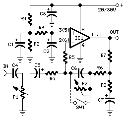
The preamplifier in question is engineered to interface with various audio devices such as CD players, tuners, and tape recorders. Its primary function is to provide an alternating current (AC) voltage gain of 4, an attribute that allows it to...
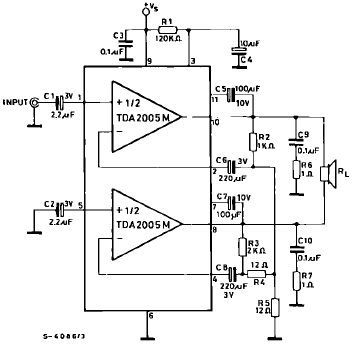
The TDA2005 is a Class B dual audio power amplifier package specifically designed for car radio applications. It facilitates the easy design of car radio power boosters. The TDA2005 power amplifier is engineered to deliver high-quality audio output in automotive...
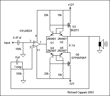
The EDFET drives like a FET, but with the bias stability of bipolar. Amps of output current can be controlled by milliamps of input current. The current gain is a design choice dictated by bandwidth. Two of things you...
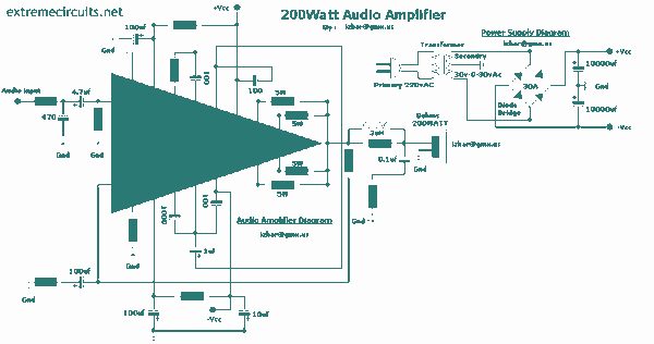
This complete high quality, low noise mono audio power amplifier is based around the Hybrid Integrated Circuit STK4050 manufactured by Sanyo. The circuit incorporates volume and has a maximum music output power of 200W. The circuit incorporates an on...
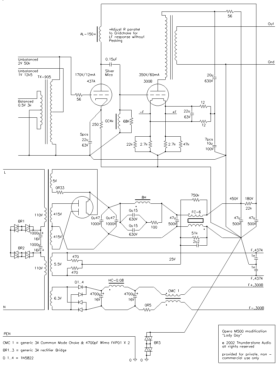
A request for a DIY 300BSE power amplifier schematic is made, with a specification to utilize Lowther PM6 speakers. The 300BSE power amplifier is a well-regarded audio amplification circuit known for its warm sound and high fidelity, particularly suited for...
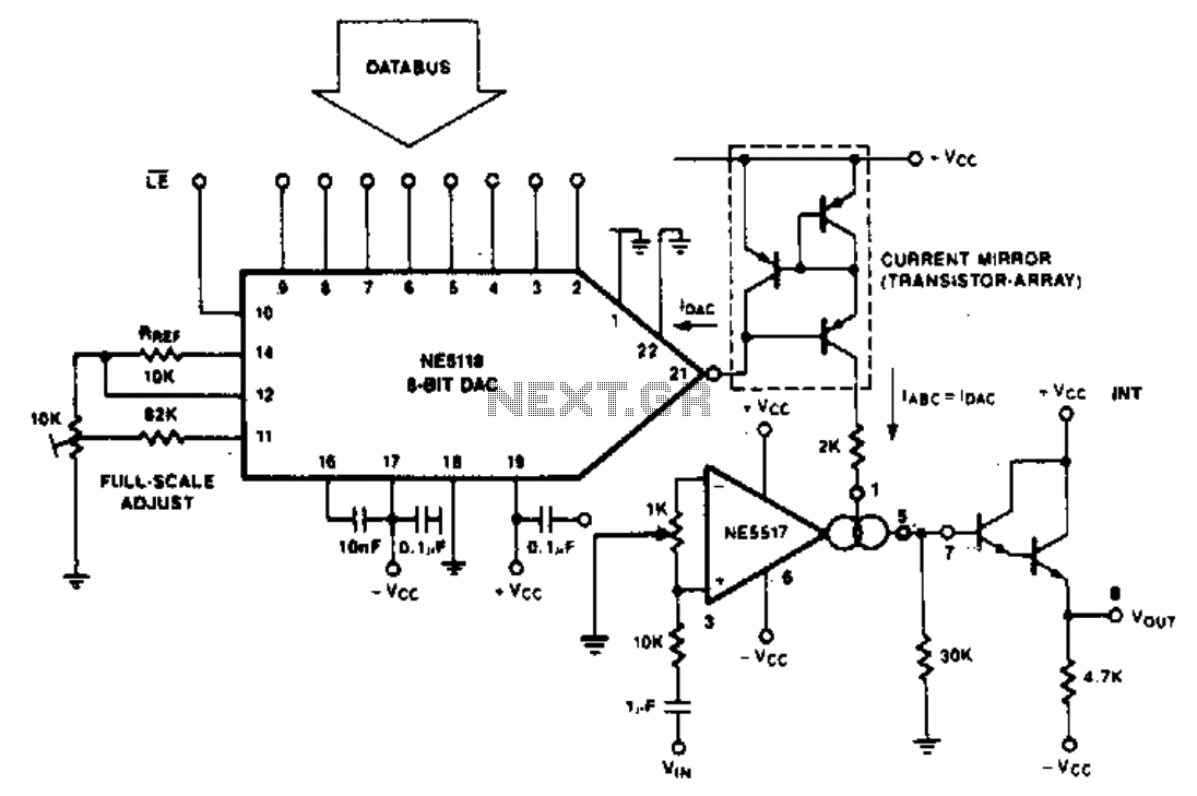
The purpose of the following application is to demonstrate how the NE5517 operates in conjunction with a DAC. The application utilizes the NE5118, an 8-bit DAC with current output, featuring an input register that makes this device fully micro-compatible....