
Fet Buffer for amplifiers
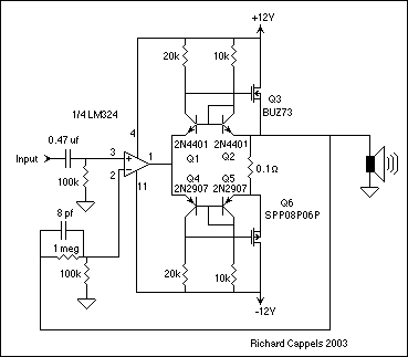
The EDFET (Enhanced Depletion-Mode Field-Effect Transistor) operates as a sophisticated output stage in audio amplifier applications, leveraging the advantages of both FETs and bipolar transistors. The architecture typically consists of a complementary buffer design, which includes two unity gain buffers: one for positive output and the other for negative output. This configuration effectively mitigates crossover distortion and enhances bandwidth due to the feedback mechanisms employed within the output stage.
In the positive-driving section, the input signal is applied to the emitter of the inverting transistor (Q1). The output of the amplifier is adjusted to account for the base-emitter voltage drop of Q1 through a diode-connected transistor (Q2). This ensures that the output signal accurately tracks the input signal while maintaining thermal stability, as the buffer's offset is influenced by the emitter current mismatch between Q1 and Q2, which is temperature-dependent.
The biasing of the output stage is critical for achieving low distortion and stable operation. The quiescent current is determined by the offsets in both the positive and negative stages, divided by a source resistor. The selection of resistor values, particularly the collector resistors (R1) and bias resistors, plays a pivotal role in establishing the desired quiescent point. Typically, equal resistor values are chosen to maintain symmetry and thermal stability.
In practical applications, it is common to see configurations where the bias current is set using a single source resistor, particularly in high-frequency scenarios where capacitive loads are prevalent. The design considerations include ensuring that the maximum output voltage and power supply voltages are compatible with the selected FETs, such as the BUZ73, which has a specified input capacitance.
The operational parameters, such as maximum gate voltage and desired frequency response, are essential for maintaining the integrity of the amplifier's performance. For example, a target frequency intercept of 2 MHz is often selected to ensure adequate phase margin, particularly in wideband applications. By carefully managing the quiescent bias and component selection, designers can achieve a robust and reliable output stage that exhibits minimal distortion and enhanced stability across varying operational conditions.The EDFET drives like a FET, but with the bias stability of bipolar. Amps of output current can be controlled by milliamps of input current. The current gain is a design choice dictated by bandwidth. Two of things you have to consider when adding a power output stage to an op-amp circuit are the frequency response and the cross-over distortion in that stage. This is especially true with wide band amplifiers, where the unity gain crossover needs to be at several hundred kilohertz.
The stage is driven much the same as a complimentary pair output stage, but with the current gain that comes with using FETs., and with feedback within the output stage that that extends the buffer's bandwidth and regulates the quiescent current. More predictable operation allows the designer to design a circuit lower overall power dissipation and better closed loop stability.
The EDFET complimentary buffer is made up of a pair of unity gain buffers, one that drives in the positive direction and the other that drives in the negative direction. Pictured above is the positive driving half of the output stage. Gain to make the output signal track the input signal comes from inverting transistor, Q1. The input signal is applied to the emitter of Q1 and the output of the amplifier is raised one diode drop to match the forward base-emitter drop of Q1, by diode connected transistor Q2.
The buffer's offset is determined by the log of the magnitude of the mismatch in the emitter currents in Q1 and Q2, and it is directly proportional to the absolute temperature. Since the saturation current usually isn't published for the transistors this expression is only usefully for appreciating the dependence of junction voltage on current and temperature.
You can come up with your own value of I0 for a given transistor if you know all the other parameters and solve the above formula for I0. By the way, since, for most practical uses, you will be running at more than a thousand times the saturation current, the "+1" term can be dropped from practical calculations.
As an example, for the audio amplifier using a EDFET buffer shown in Figure 1. The following assumptions are applied: The maximum output voltage is 5 VDC with respect to ground, the power supply (VA) is 12 VDC, the maximum gate voltage is 8 VDC, the input capacitance, Ciss of the BUZ73 is 500 pf, and an intercept of 2 MHz is desired so as to have plenty of phase margin (for the largest frequency difference between the point the closed loop response of the amplifier reaches 00 dband the point that the FET buffer starts to roll off). The bias current is set in a manner similar to the classic complimentary pair. I am only using one source resistor to set the bias current. In some high frequency applications in which a capacitive load is being driven (for example, a 50 video amplifier) the waveform symmetry would be preserved by splitting the resistor and taking the output signal at the tap as shown in the classic complimentary pair, but for applications one is likely to be using power MOSFETs for, it is unlikely that a second resistor would do more than fulfill an emotional need to make the circuit look symmetric.
The quiescent point source current is equal to the sum of the offsets in the postive-driving and negative-driving parts of the stages divided by the source resistor. The way I set the quiescent bias is to first select the collector resistors (R1 in the schematic of the single ended buffer), and then pick the bias resistors.
In the circuit above, using 1 k resistors to bias the diode connected transistors and 2 k resistors for the collector loads on the inverting stage (as shown) the output stage is just barely into conduction, drawing a few hundred mircoamps. This is near the zero bias point at which the bias current should vary little with temperature. Increasing the 1k resistors (R2) would increase the quiescent current. When the junctions are biased for zero volts offset, the temperature coefficient of the offset becomes zero (Ideally).
For a low distortion class B stage, this is the bias point to shoot for. The starting point is to use equal value resistors for R1 and R2. As the base-emitter voltage of Q2 decreases, the quiescent current (current when not driven) through the output stage will increase. 🔗 External reference
Related Circuits
The sound system features a de-sensitized design with a maximum range that can be increased if desired. It includes two tone controls: one offering a lift of 10 dB and the other providing a subtle cut of 3 dB....
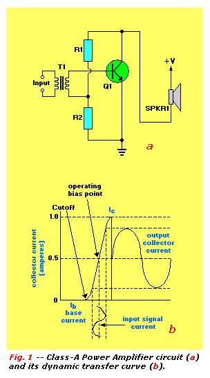
An audio power amplifier can enhance weak signals from devices like tuners, CD players, or tape decks to fill a room with sound. This article emphasizes the operating principles and circuitry of low-frequency power amplifiers utilizing bipolar junction transistors...
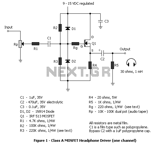
The circuit described in this article is a MOSFET follower for driving headphones. FET followers can supply high current, but have a voltage gain of slightly less than unity. They are most suitable in applications where the input signal...
Capacitors C1 and C2, in conjunction with a speed controller, function by receiving voltage at the gate of the MOSFET. When the voltage on C is applied, it activates the operation of the MOSFET. In this circuit configuration, capacitors C1...
Most amplifiers operate at acoustic frequencies, sometimes requiring two or even three transformers instead of a single power transformer. This approach is more prevalent in high-end amplifiers, where enthusiasts often prioritize high fidelity over cost. In these setups, the...
.jpg)
Sealed lead-acid batteries are commonly used in power electronics applications, including uninterruptible power supplies (UPS), inverters, and emergency lamps. They provide power to the load when utility power is unavailable. Upon restoration of utility power, a charger supplies power...
Warning: include(partials/cookie-banner.php): Failed to open stream: Permission denied in /var/www/html/nextgr/view-circuit.php on line 713
Warning: include(): Failed opening 'partials/cookie-banner.php' for inclusion (include_path='.:/usr/share/php') in /var/www/html/nextgr/view-circuit.php on line 713