
555 Fm Circuit Circuit
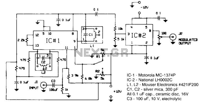
The circuit described is designed to apply a direct current (DC)-coupled frequency modulation (FM) or pulse position modulation (PPM) to a 555 timer integrated circuit (IC) configured as an oscillator. The primary components include two integrated circuits: the Motorola MC-1374P (IC-1) and the National LH0002C (IC-2).
Inductors L1 and L2 are specified as Mouser Electronics #421IF200, which are suitable for RF applications. These inductors play a critical role in tuning the circuit to the desired frequency response. Capacitors C1 and C2, both silver mica with a capacitance of 300 pF, are used for stability and frequency tuning, while the additional capacitors, all rated at 0.1 µF and 16V, are ceramic disc types, providing decoupling and filtering within the circuit. C3, an electrolytic capacitor rated at 100 µF and 10V, is likely used for power supply filtering or timing applications.
Adjustment procedures are critical for achieving the desired output characteristics. The resistor R1 should be adjusted to minimize the carrier signal, ensuring that the output from the function generator generates a peak-to-peak voltage of 500 mV at pin 8 of IC-2, which is indicative of a suppressed carrier double sideband amplitude modulation. Further, R2 and the function generator level must be adjusted to reach an output of 800 mVpp at the same pin, which corresponds to standard amplitude modulation with an active carrier.
Fine-tuning of the circuit is also necessary. L2 should be adjusted to resonate at 455 kHz, a common intermediate frequency in AM radio applications. Finally, L1 should be tuned for maximum output, ensuring optimal performance of the oscillator circuit. This setup can be employed in various applications, including signal processing and communications, where precise modulation techniques are required. Circuit for applying a dc-coupled FM or PPM to a 555 configured as an oscillator. IC-1 - Motorola MC-1374P. IC-2 - National LH0002C. L1, L2 - Mouser Electronics #421IF200. C1. C2 - Silver mica, 300 pF. All 0.1 uF cap., ceramic disc, 16V. C3 - 100 uF, 10 V, electrolytic ADJUSTMENT: Adjust R1 for minimum carrier; signal from function generator should generate 500 mVpp at pin 8 of IC-2 (suppressed carrier double sideband). Adjust R2 and function generator level-to achieve 800 mVpp at pin 8 of IC-2 (standard AM with carrier).
Adjust L2 for 455 kHz. Adjust L1 for maximum output. 🔗 External reference
Related Circuits
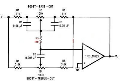
A simple tone control circuit can be designed using the LM833 operational amplifier along with a few external components. The LM833 is a dual general-purpose operational amplifier, specifically optimized for performance in audio applications. This tone control circuit utilizes...
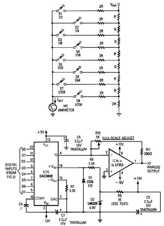
Figure A illustrates an R/2R resistor ladder. Each closed switch increases the current output. A basic channel A/D converter is depicted in Figure B. The voltage reference (D2) is shared among all channels, while the value of the dropping...
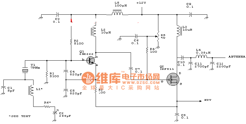
The circuit diagram of a TV antenna is sourced from the technical information provided by Chinaicmart. For more detailed information or additional circuit designs, further inquiry may be necessary. The circuit diagram for a TV antenna typically consists of several...
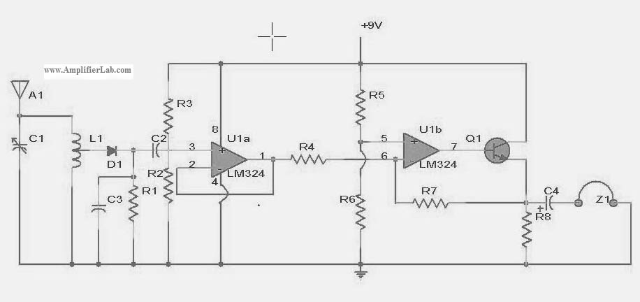
The following circuit illustrates a power amplifier electronic circuit, specifically a tube audio RF amplifier circuit diagram. This circuit is based on the LM324 integrated circuit. The power amplifier circuit utilizing the LM324 operational amplifier is designed to enhance audio...
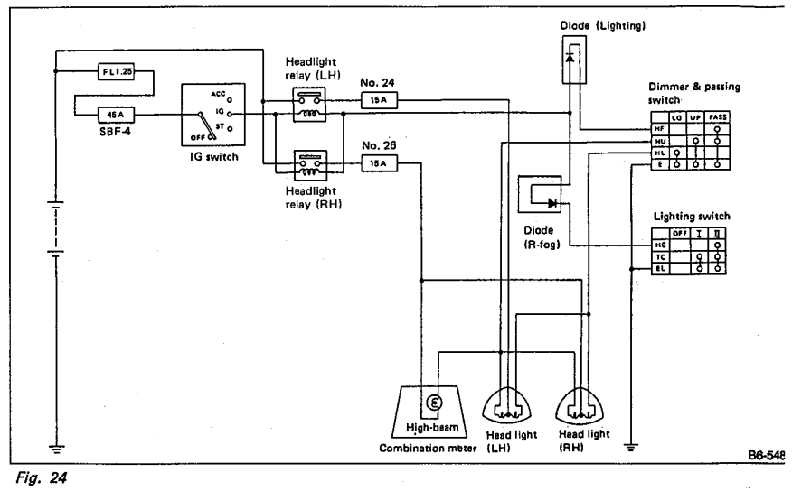
Understanding the headlight wiring in a car involves examining the purpose of two diodes in the circuit diagram. The circuit allows for two independent methods of activating the light relays: through the light switch or by flashing the high...
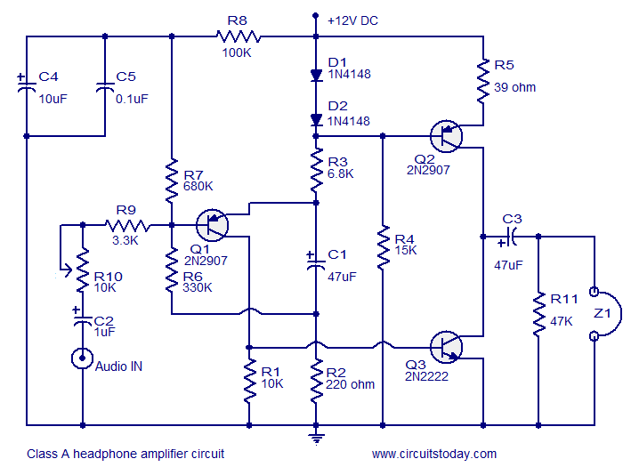
Transistor amplifier circuits that are simple and easy to construct. This includes a headphone amplifier, a four-transistor amplifier, and a low-power amplifier. Transistor amplifier circuits are fundamental components in electronic design, offering various applications ranging from audio amplification to signal...
Warning: include(partials/cookie-banner.php): Failed to open stream: Permission denied in /var/www/html/nextgr/view-circuit.php on line 713
Warning: include(): Failed opening 'partials/cookie-banner.php' for inclusion (include_path='.:/usr/share/php') in /var/www/html/nextgr/view-circuit.php on line 713