
555 monostable circuit diagram of a low power consumption

This circuit utilizes a combination of NAND gates and a 555 timer in a CMOS configuration to create a versatile timing application. The four 2-input NAND gates are arranged to form the necessary logic for the flip-flop configuration, which can be either set or reset based on the input signals. The low power consumption characteristic is particularly beneficial for battery-operated devices or applications where energy efficiency is critical.
The CD4011 is a quad 2-input NAND gate IC, which provides the required logic functions. In this circuit, it is instrumental in forming the RS flip-flop, a fundamental building block in digital electronics that can store a single bit of data. The flip-flop's output state is determined by the inputs, allowing for either a high or low state, which is essential for timing applications.
The timing aspect of the circuit is governed by the RC time constant, which is calculated using the formula Td = 1.1R1C1. Here, R1 is the resistance in ohms, and C1 is the capacitance in farads. This relationship indicates that the duration of the output pulse is directly influenced by the values of the resistor and capacitor used in the circuit. By adjusting these components, the pulse width can be fine-tuned to meet specific timing requirements.
In summary, this circuit design effectively integrates NAND gates and a CMOS 555 timer to create a low-power, reliable timing solution. The closed-loop configuration and the use of the RC time constant for timing control enhance its functionality, making it suitable for various electronic applications where precise timing and minimal power usage are essential. As shown, the circuit including a four 2-input NAND gate and a CMOS CD4011 type 555, and thus the output of either a static or high-time period, the power consumption is minima l. CD4011 3 door, 4 door composition RS flip-flop. Since the entire circuit in a closed loop, the timing depends on the RC time constant of the pulse width, i.e., Td 1.1R1C1.
Related Circuits
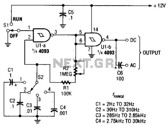
The circuit illustrated operates within a frequency range of 2 Hz to 30 kHz. Additionally, R2 is configured as either a linear or logarithmic potentiometer. The circuit is designed to accommodate a wide frequency spectrum, making it suitable for various...
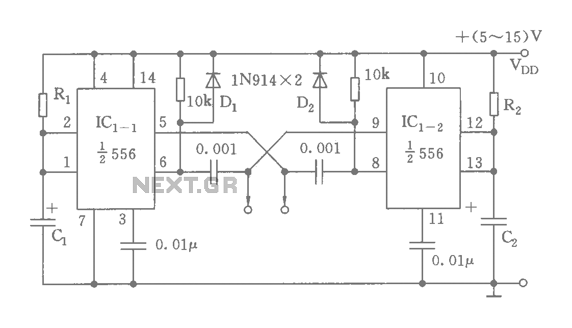
The circuit features a dual time base using a 556 timer, which comprises two synchronized multivibrators and two output clock signals. The output signals are synchronized with defined intervals, and the oscillation frequency can be adjusted by varying the...
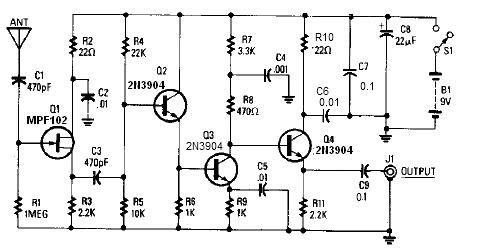
A simple active antenna can be designed using this electronic circuit diagram. This active antenna utilizes transistors and a few common electronic components. In the practice of short-wave frequency reception, a general rule is that a longer antenna will...
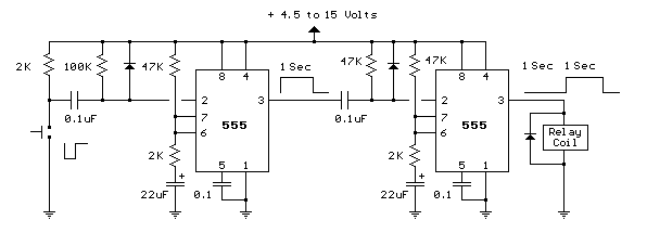
The circuit below demonstrates the generation of a single positive pulse that is delayed in relation to the trigger input time. It is similar to a previously described circuit but utilizes two stages, allowing for control over both the...
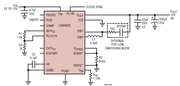
A very simple, high-efficiency switching mode buck-boost power supply circuit can be designed using the LTM4609 switching regulator IC. This circuit will provide a fixed output voltage of 12 volts. As illustrated in the schematic, the switching power supply...
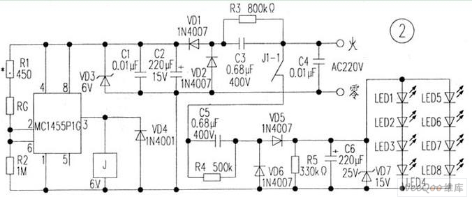
The circuit is depicted in Figure 1, while the electrical schematic diagram is presented in Figure 2. The AC voltage of 220V is reduced by components C3 and R3. The diodes VD1 and VD2 rectify the voltage, and capacitors...