
14-20dB gain simple active antenna circuit diagram
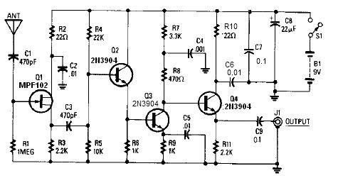
The active antenna circuit outlined is designed to enhance the reception of RF signals, particularly in the short-wave band. The circuit typically includes a few key components: transistors, resistors, capacitors, and a JFET. The JFET serves as the primary amplification device, leveraging its high input impedance and low output impedance characteristics to maximize signal gain while minimizing signal loss.
The transistors Q2, Q3, and Q4 work in a cascading configuration to amplify the received signal. Q2 acts as the initial amplifier, receiving the weak RF signal from the antenna. The output from Q2 is fed into Q3, which further amplifies the signal. Q4 then converts the output from Q3 into a lower impedance, suitable for matching with a standard 50-ohm input of most receivers. This impedance transformation is crucial for ensuring maximum power transfer and efficient signal reception.
The circuit may also incorporate bypass capacitors to stabilize the power supply and filter out any unwanted noise, ensuring a clean signal is delivered to the receiver. The gain characteristics of the circuit are designed to provide optimal performance across a range of frequencies, making it versatile for various short-wave applications.
In summary, this active antenna circuit is a practical solution for those needing enhanced signal reception without the space for a larger antenna. Its design allows for effective impedance matching and signal amplification, making it suitable for a wide range of short-wave frequencies.A very simple active antenna can be designed using this electronic circuit diagram. This active antenna is based on transistors and other few common electronic components. Because in practice of frequency short-wave reception, the general rule is that if the used antenna is longer, the stronger the received signal will be we need in some cases ( when we can not built a big antenna, because of some factors ). Antennas that are much shorter than 1/4 wavelength present a very small and highly relative impedance that is dependent on the received frequency. It is difficult to match impedances over a decade of frequency coverage. For this RF circuit a gain of 20dB is typical from 1-18 MHz, decreasing to 14dB at 30MHz. For this active antenna circuit many different types of JFET`s may be used, such as the MPF102, NTE451, ECG451 or 2N4416 and 2N3904 or 2N2222 transistor works well for Q2, Q3, and Q4.
Transistor Q4 transform Q3`s relatively moderate output impedance into a low impedance, thereby providing sufficient drive for a receiver`s 50-ohm antenna-input impedance. 🔗 External reference
Related Circuits
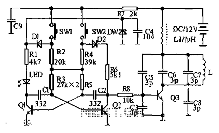
The circuit diagram illustrates a dual radio remote control switch system. The transmitter section features Q3, which generates a high-frequency carrier signal, while Q1 and Q2 form the oscillator circuit. Pressing switch SW1 results in an oscillation frequency of...
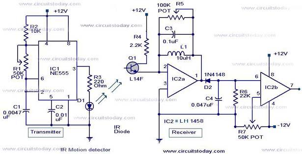
Infrared (IR) Motion Detector Circuit featuring a motion detector alarm and an infrared sensor. The circuit diagram and its operation are provided in detail. The infrared (IR) motion detector circuit is designed to detect motion within a specified range and...
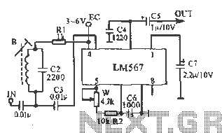
This figure illustrates the schematic of the LM567 SCA broadcast reception information machine. The LM567 serves as a narrow-band phase-locked loop designed primarily for SCA broadcast demodulation. The configuration includes a potentiometer (W) and capacitor (C6) that determine the...
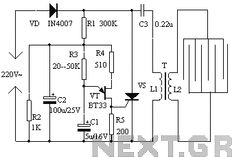
The electronic fly disinfestation system is a simple and effective device designed to eliminate flies using electrical means. The apparatus, as depicted in Figure 1, operates on 220V mains power supplied directly through a rectifier. It utilizes a relaxation...
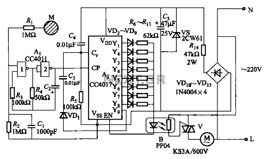
The circuit depicted in Figure 3-7 utilizes a touch sensor chip in conjunction with a conductive sheet. It is designed to achieve eight different speed settings. The CC4011 timing pulse oscillator is comprised of an integrated circuit. The configuration...
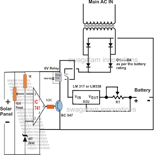
The automatic changeover relay circuit was requested by Mr. Karimulla Baig. The circuit is designed to charge a connected battery at a constant current using power from a solar panel. In the absence of solar energy, such as during...