
555 timer circuit diagram of a group of anti-jamming

The 555 timer IC is a versatile component widely used in various electronic applications, particularly for generating precise timing intervals and pulse-width modulation. In this specific monostable configuration, the circuit is designed to produce a single output pulse in response to an external trigger. The simplicity of the design allows for easy integration into larger systems while providing reliable performance.
The forced reset mechanism implemented through pin 4 enhances the circuit's immunity to noise and unwanted signals, ensuring that the timer only operates when intended. The inclusion of a transistor (VT1) allows for the control of the output state based on the state of button B, providing a straightforward user interface for activating the timer.
The choice of components plays a crucial role in the circuit's reliability and performance. The use of carbon film resistors ensures stable resistance values, while the ceramic and electrolytic capacitors are selected to meet the timing requirements of the circuit. Diodes are chosen based on their switching characteristics and voltage ratings to ensure fast response times and prevent back EMF from affecting the circuit operation.
Overall, this 555 timer-based monostable circuit is an effective solution for applications requiring precise timing control, and its robustness against interference makes it suitable for various electronic projects.555 in the use of time-based circuit design from the timer circuit, generally will be 555 monostable circuit is connected, so connected so that the circuit design is simple, re quires only a few resistors and capacitors can be achieved triggering but there are also external interference on 555 feet of 2-based circuit, the circuit clever use of 555 feet of forced reset circuit 4 functions to achieve interference timer circuit. This circuit is tested and functionable. When SB is disconnected, 555 feet by 4 circuit resistor R6 is connected to ground, the circuit 555 is forcibly reset.
At this time, no matter how much interference by 2 feet, 555 circuits do not work. When you press button B, the power supply through a diode VD1 is applied to 4 feet high, forced reset circuit release function group, while power supply through a resistor R1 is applied to the base of transistor VT1, VT1 conduction so that the capacitor C2 is connected to VT1 through the collector to a low level output circuit IC 2 feet, IC flip set, 3 feet high output, LED lights, the relay K is energized, contact K-1 closed, outlet External power supply, and 3 feet high by VD2 such a high self-locking circuit output to 4 feet. After the end of the transient, the circuit turn back to steady state, 3 feet output low, the relay K energized, contacts K-1 off, the circuit returns to the initial state.
Component selection: IC1555 timebase circuit used when NE555, A555, SL555 and other base integrated circuit; R1 ~ R7 selected RTX-1/4W carbon film resistors; RP available WSW organic solid variable resistor trimming; C2, C4, C5, C6 selection CT1 type ceramic capacitors, C1, C3, C7 selection CD11-16V electrolytic capacitors; diode VD1, VD2, VD3 selected IN4148 silicon switching diodes, VD4 ~ VD7 selected IN4001 silicon ordinary rectifier diode; relay K You may need to select electrical equipment; three-terminal integrated voltage regulator type selection 7809 three-terminal voltage regulator integrated circuit.
Related Circuits
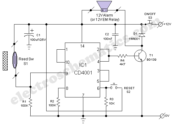
Have you ever accidentally left your front door ajar and had a pet escape? Here is a smart solution to this problem. The circuit is relatively simple but serves as a great example of using a compact circuit to...
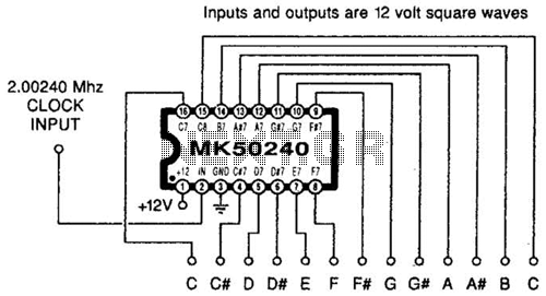
Using an MK50240, this circuit generates 12 top octave tones. The input and output lines can be separated using a binary divider IC to achieve the lower notes. Inputs and outputs are 12-volt square waves. The MK50240 is a specialized...
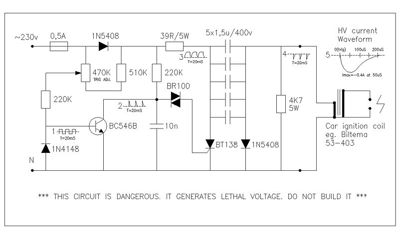
This circuit generates high voltage pulses from a 230 VAC line voltage. The drive end's swing comparator circuit was developed by the creator of this page. The working end is derived from a stroboscope trigger supply circuit. All circuits...
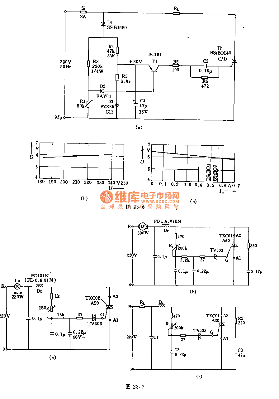
This is a non-contact power regulator circuit designed for a light load. By adjusting a 150kΩ potentiometer, phase shift can be achieved, and a trigger voltage is applied to the gate of a bidirectional thyristor through a bidirectional trigger...
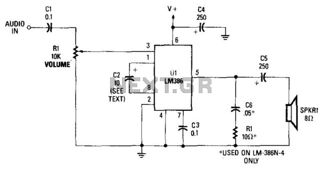
This simple receiver AF amplifier can supply several hundred milliwatts to an 8-ohm speaker. The gain is approximately 200X. If high gain is not required, C2 can be removed, resulting in a gain of 20. R1 and C6 are...

The TDA4863J basic application circuit operates with a positive supply voltage (VP), a flyback power supply voltage (VF), and a negative supply voltage (VN). The input signal is provided from the sawtooth signal input at pins 6 and 7,...