
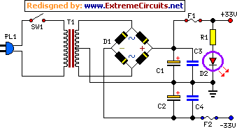
5V Power Supply Circuit Using Overvoltage Protection

The power supply circuit is designed to ensure the protection of TTL ICs from overvoltage conditions by employing a crowbar protection scheme. The circuit includes a transformer with a primary winding rated for 230V AC and a secondary winding that outputs 12V at 2A. This transformer steps down the high voltage AC supply to a lower voltage suitable for the TTL ICs.
The key components of the circuit include a zener diode (D2), which serves as a voltage reference. When the output voltage exceeds 5.6V, the zener diode begins to conduct, triggering the triac (T1). The triac is a semiconductor device that can control large amounts of current with a small gate trigger. Once activated, T1 creates a short circuit across the power supply, effectively cutting off the voltage supplied to the load and allowing the fuse to burn out, thereby protecting sensitive components.
The trip voltage, which determines when the circuit will activate the triac, can be adjusted by changing the resistance value of R2 or the zener diode D2. This flexibility allows for fine-tuning of the circuit to accommodate different load conditions or specific requirements of the application.
The use of a fuse in conjunction with the triac provides a fail-safe mechanism. While the fuse typically takes longer to react, the immediate action of the triac ensures that no harmful voltage is present during this delay. The design emphasizes reliability and safety, making it suitable for environments where TTL ICs are used.
Capacitors in the circuit must be rated for at least 25V to handle potential voltage spikes without failure. If a pre-assembled bridge rectifier rated at 1A is not available, it can be constructed using four 1N4007 diodes, which are standard rectifier diodes known for their robustness and reliability in various applications. This design ensures that the power supply circuit remains effective and safe for use with TTL ICs and similar sensitive electronic components.This is a design for power supply circuit. This circuit can produce source voltage 5V. This circuit is built by TTL IC`s. But this design is simple design. This is the figure of the circuit. For circuits using TTL ICs the supply voltage is a great concern and a slight increase in supply from the rated 5V may damage the IC. Using fuses alone does n ot solve the problem because a fuse may take several milliseconds to blow off and that`s enough time for the IC to get damaged. In this circuit a crowbar scheme is used in which a triac short circuits the power supply and burns the fuse.
The burning time of the fuse is not a concern because the power supply is already shorted by the triac and the output voltage will be zero. Operation of the circuit is when the output voltage exceeds 5. 6 volts the zener diode D2 conducts and switches ON the triac T1. Now T1 acts as a closed switch, shorting the circuit. The output voltage drops to zero and fuse gets burned off. The trip voltage can be varied by varying the values of D2 and R2. Since the switching of triac takes place within few micro seconds there will be no damage to the TTL ICs or any other such voltage sensitive components in the load circuit.
For the transformer T1 can be a 230 V AC primary, 12v secondary, 2A step-down transformer. All capacitors must be rated at least 25V. If 1A Bridge is not available, make one using four 1N4007 diodes. 🔗 External reference
Related Circuits
The goals were achieved by utilizing a discrete-components operational amplifier (op-amp) driving a complementary common-emitter output stage configured for Class B operation. In this configuration, for small output currents, the output transistors remain off, allowing the op-amp to supply...

A normally open pushbutton switch (SI) provides a positive input pulse to pin 4 of U1, activating the integrated circuit (IC). The output from U1 at pin 6 delivers base-drive current to a Darlington pair consisting of Q1 and...

The high-pressure direct current power supply has become increasingly widespread. This system outputs in parallel with double-channel power to achieve low ripple direct current. In situations where gas switching tube frequency is limited, this method can generate low ripple...

Carrier current remote control device or intercom circuit diagram as follows: The circuit diagram for a carrier current remote control device or intercom system typically involves the use of carrier current technology to transmit audio signals over existing electrical...

A variable resistor is utilized to adjust the light-level response of a phototransistor. Phototransistors exhibit higher light sensitivity compared to photodiodes; however, they typically demonstrate a lower frequency response. A variable resistor, often referred to as a potentiometer or rheostat,...
The following circuit illustrates a fire alarm circuit diagram utilizing the NE555 integrated circuit (IC). Features include functioning as a heat sensor and incorporating a 10 kilo-ohm resistor. The fire alarm circuit based on the NE555 IC is designed to...