
60 Watt Audio Power Amplifier
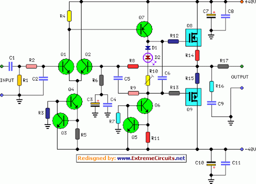
The circuit utilizes a topology that is designed to maximize performance through the careful selection of components. The IRFP240 and IRFP9240 MOSFETs are known for their high power handling capabilities and thermal stability, making them suitable for high-fidelity audio applications. The choice of high-voltage Motorola transistors in the earlier stages ensures that the signal amplification is robust, providing low distortion and high linearity.
Operating at a supply voltage of ±40V is a prudent choice, as it balances performance and safety. However, by allowing for an increase to ±50V, the design opens up opportunities for higher output power, making it suitable for driving larger speakers or achieving higher sound pressure levels in larger spaces.
The modification of replacing two diodes with a red LED in the quiescent current path is a notable enhancement. This change not only improves thermal stability but also provides a visual indicator of the amplifier's operational status, which can be beneficial during setup and testing.
In terms of power supply capacitors, C1 and C2 are critical in maintaining voltage stability during operation. Increasing the capacitance to 10,000 µF for stereo configurations helps to ensure that the amplifier can respond quickly to dynamic changes in audio signals without introducing unwanted noise or distortion.
Grounding is a vital aspect of audio circuit design. Proper grounding techniques help to minimize the risk of hum and ground loops, which can significantly degrade audio quality. The specified grounding scheme ensures that all components share a common reference point, reducing the likelihood of interference.
Overall, this circuit design exemplifies a well-thought-out approach to high-performance audio amplification, with careful attention paid to component selection, power supply requirements, and grounding practices.Circuit topology is about the same of the above mentioned amplifier, but the extremely rugged IRFP240 and IRFP9240 MosFet devices are used as the output pair, and well renowned high voltage Motorola`s transistors are employed in the preceding stages. The supply rails voltage was kept prudentially at the rather low value of + and - 40V. For those wishing to experiment, the supply rails voltage could be raised to + and - 50V maximum, allowing the amplifier to approach the 100W into 8 Ohm target: enjoy! A matching, discrete components, Modular Preamplifier design is available here: Modular Audio Preamplifier.
In the original circuit, a three-diode string was wired in series to R10. Two of these diodes are now replaced by a red LED in order to achieve improved quiescent current stability over a larger temperature range. Thanks to David Edwards of LedeAudio for this suggestion. The value suggested for C1 and C2 in the Power Supply Parts List is the minimum required for a mono amplifier.
For optimum performance and in stereo configurations, this value should be increased: 10000 µF is a good compromise. A correct grounding is very important to eliminate hum and ground loops. Connect to the same point the ground sides of R1, R3, C2, C3 and C4 and the ground input wire. Connect R7 and C7 to C11 to output ground. Then connect separately the input and output grounds to the power supply ground. Be the first of your friends to get free diy electronics projects, circuits diagrams, hacks, mods, gadgets & gizmo automatically each time we publish.
Your email address & privacy are safe with us ! 🔗 External reference
Related Circuits
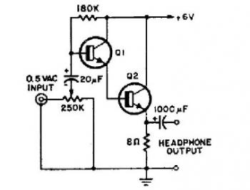
This schematic diagram illustrates a simple headphone amplifier circuit constructed using two NPN transistors. Suitable transistor options include the BC549C, as well as other NPN transistors such as the European equivalents BC548C, BC547C, BC239, 2N5818, or 2N2222. An audio...
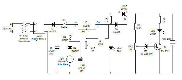
Battery charger utilizing solar and electrical power with a circuit diagram. This dual power source battery charger can charge a lead-acid battery using two different power sources. The battery charger circuit is designed to efficiently charge a lead-acid battery by...

The 78W series voltage regulators are designed to handle an input voltage of approximately 35V, while the 24V type can withstand up to 40V. It should be noted that these regulators will not operate effectively with a significant input-output...
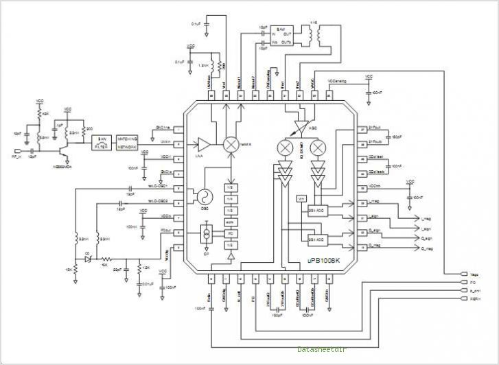
The PB1009K is a silicon monolithic integrated circuit (IC) designed for GPS receivers. This IC incorporates a complete voltage-controlled oscillator (VCO), a second intermediate frequency (IF) filter, a 4-bit analog-to-digital converter (ADC), and a digital control interface, all aimed...
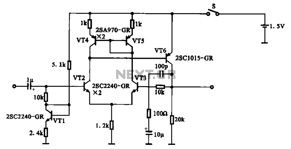
A 1.5V-powered microphone signal amplifying circuit is designed with a power supply for the microphone signal amplification. The circuit primarily consists of a differential amplifier formed by transistors VT2 and VT3. Additionally, VT6 functions as a common emitter voltage...
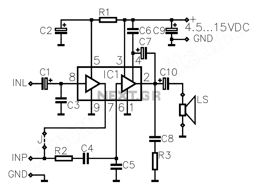
The circuit diagram presented is for a compact mini audio power amplifier that operates with a DC supply voltage ranging from 4.5 volts to a maximum of 18 volts. This amplifier utilizes the TDA1015 integrated circuit, produced by NXP...