
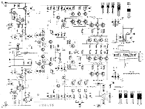
8 LED Effects using PIC16F84A
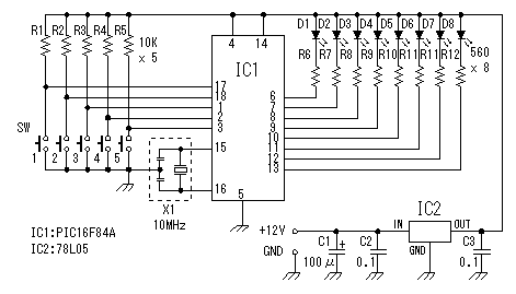
Eight feet by RV7 RV0 used as outputs - drivers Led. Among them inserted 560R resistors, which limit the current flowing through the output pins and protect them from destruction. The descent of the led associated with resistance and rise to 5V. When the output is in a foot (HI +5 V) the led is not lit and when it is (LOW 0V) glows. In this example, we used high brightness led to reduce the current flowing through each leg.
Timing Circuit
For the timing of the processor used a ceramic filter (Resonator) or 10MHz crystal and two 22pF ceramic capacitors
Feeder circuit
The IC2 stabilizes the voltage from 12VDC to 5VDC and capacitors to smooth and filter. Since the consumption of the circuit is too low a stabilizer of about 100mA is enough.
Five pins, designated as RA0 to RA4, function as digital inputs within this circuit. These pins are configured with a pull-up resistor of 10kΩ connected to a +5V supply. When no switch is pressed, each pin maintains a high logic level (+5V). Upon pressing any switch, the corresponding pin is pulled to a low logic level (0V). A phenomenon known as switch bounce occurs during this action, where the mechanical contacts of the switch may rapidly open and close, causing multiple transitions between high and low states. In this design, debounce logic is not implemented, allowing the microprocessor to immediately respond to the first detected low state, initiating the corresponding routine.
The output section of the circuit includes eight pins, labeled RV0 to RV7, which are used to drive LEDs. Each output pin is connected in series with a 560Ω resistor, which serves to limit the current flowing through the LEDs, thereby preventing damage to the output pins. The LED operation is such that when the output pin is driven high (+5V), the LED remains off, while a low output (0V) causes the LED to illuminate. High-brightness LEDs are utilized in this configuration to ensure visibility while minimizing the current drawn from each output pin.
For timing purposes, the circuit employs a ceramic resonator or a 10MHz crystal oscillator, accompanied by two 22pF ceramic capacitors. This configuration ensures stable clock signals necessary for the microprocessor's operation.
The power supply circuit includes an integrated circuit (IC2) that regulates the input voltage from 12VDC down to a stable 5VDC output. Additional capacitors are used in the circuit to smooth and filter the voltage output, providing a stable power supply for the microprocessor and associated components. Given the low power consumption of the circuit, a voltage regulator rated for approximately 100mA is sufficient to meet the operational requirements.Five pins RA0 to RA4 are used as inputs. The pins are connected to the 5V average resistance 10K (Pull-up). So when no switch is not depressed all the pins have a high potential (HI +5 V). When one of them is pressed then the foot is connected to get a low potential (LOW 0V). When a switch is pressed, then the phenomenon of 'Bounce' (Debaunce), this is because the switch does not always close the circuit but once more (rebounds) leading the microprocessor takes several input signals. In our example code is not used to prevent rebound as soon as one pressed the switch immediately begins the routine imaging of the selected effect which is greater than this year's rebound.
Circuit output (Driving Led) Eight feet by RV7 RV0 used as outputs - drivers Led. Among them inserted 560R resistors, which limit the current flowing through the output pins and protect them from destruction. The descent of the led associated with resistance and rise to 5V. When the output is in a foot (HI +5 V) the led is not lit and when it is (LOW 0V) glows. In this example we used high brightness led to reduce the current flowing through each leg. Timing Circuit For the timing of the processor used a ceramic filter (Resonator) or 10MHz crystal and two 22pF ceramic capacitors Feeder circuit The IC2 stabilize the voltage from 12VDC to 5VDC and capacitors to smooth and filter.
Since the consumption of the circuit is too low a stabilizer of about 100mA is enough. 🔗 External reference
Related Circuits
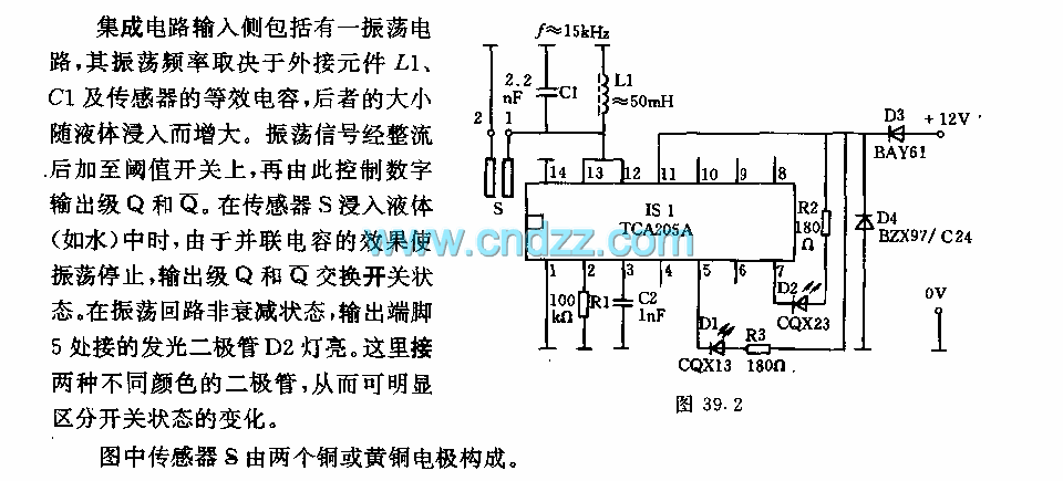
The integrated circuit input side contains an oscillating circuit, where the oscillation frequency is determined by the external components L1, C1, and the sensor's equivalent capacitance. The equivalent capacitance increases as the sensor is immersed in liquid. The oscillating...
The coil has been enhanced with additional turns, necessitating an improvement in insulation. Epoxy was chosen as the insulating material, with an increased quantity applied over the soldered connections. To ensure the reliability and performance of the coil, the additional...
More: A comprehensive electronic schematic typically includes various components such as resistors, capacitors, diodes, transistors, and integrated circuits, interconnected to perform specific functions. Each component is represented by standardized symbols, and their values are indicated alongside or...
The following circuit illustrates a 2000W Power Amplifier Circuit Diagram. This circuit utilizes the BC560C transistor. Features include a robust design. The 2000W power amplifier circuit is designed to deliver high output power suitable for various applications, including audio amplification...
Government data sets available online are often sourced from major metropolitan areas or infrastructural centers. With an easy-to-follow introduction to new software and technologies, the urban sensor kit allows anyone to obtain location-specific information and share it with a...
This is a discrete high-current switch-mode LED driver circuit. The fundamental principle of this circuit is based on the buck-converter topology. The efficiency of this circuit is 80%. The discrete high-current switch-mode LED driver circuit utilizes a buck converter configuration...