
8051 Development Board

The development board schematic is designed to facilitate the educational exploration of the 8051 microcontroller architecture and its operational capabilities. The inclusion of a bus demultiplexer (IC7) allows for efficient management of memory addresses, ensuring that both program and data memory can be accessed seamlessly. The RS232 interface (IC12) provides a means for serial communication with other devices, making it easier to debug and interact with the microcontroller during development.
The RESET and clock circuits are critical for initializing the microcontroller and maintaining its timing operations. Proper management of these signals is essential for reliable performance. The ISP connector (SV1) enables in-system programming, allowing users to update firmware without removing the microcontroller from the board.
The NAND gates (IC6C and IC6D) serve a vital role in integrating the read and program store enable signals, creating a unified control signal (RDPSEN) that governs access to the external RAM. This design choice enhances the flexibility of the board, allowing it to utilize external RAM for both program execution and data storage, thus expanding the capabilities of the 8051 microcontroller.
The choice of microcontroller in a DIP40 package provides versatility, as it supports a range of devices within the 8051 family. The jumper configuration for the EA input allows users to select between internal ROM and external memory options, catering to various application needs. This feature is particularly beneficial for developers who require specific memory configurations for their projects.
Overall, this development board serves as an effective platform for learning and experimentation with the 8051 microcontroller, providing essential features and flexibility for users to explore embedded system design and programming.This chapter contains the description of a simple development board for the study of the 8051 family of microcontrollers Unlike the development boards dedicated to the HC11 and AVR families, presented in the previous chapters, this project allows the user to load and execute programs in an external RAM area, addressed to be visible both in the p rogram memory and data memory address space. The schematic of the board is presented in Fig. 11. 1, 11. 2, and 11. 3. Figure 11. 1 shows the microcontroller IC10, the bus demultiplexer IC7, the RS232 interface IC12, the RESET and clock circuits, and the ISP connector SV1. Note the presence of the two NAND gates IC6C and IC6D, which implement the logic function AND between the signals RD (Read) and PSEN (Program Store Enable), both active LOW, and generate the signal RDPSEN.
RDPSEN is active LOW when either RD or PSEN is LOW. Connecting this signal to the RD input of an external RAM circuit allows the use of this RAM to store program as well as data. The microcontroller can be any of 8032, 8051, 8052, AT89C51, AT89C52, etc. in a DIP40 package. The input EA (External Access) of the MCU is connected to the jumper JP1 to allow the use of the internal ROM, if this is available.
Connect the jumper so that EA = 1 to use the internal ROM. When the external ROM is. 🔗 External reference
Related Circuits
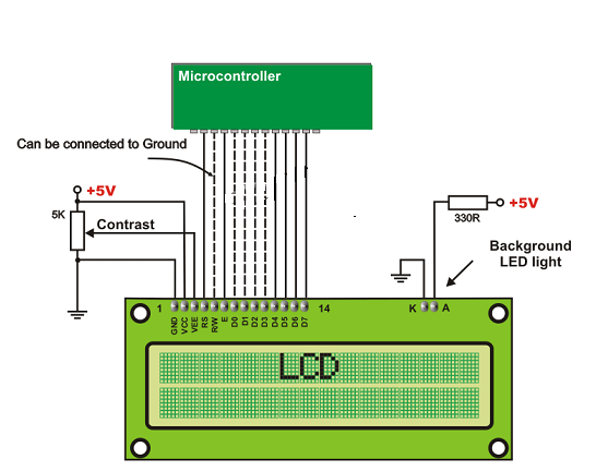
Learn how to interface a 16x2 LCD with the 8051 microcontroller. Download free source code for LCD interfacing with the 8051 microcontroller. The interfacing of a 16x2 Liquid Crystal Display (LCD) with the 8051 microcontroller is a common practice in...
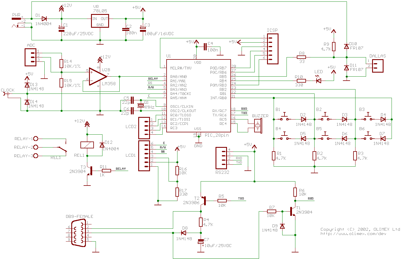
A versatile package containing numerous potential projects. This development board is designed for 28-pin PIC microcontrollers and includes a power supply circuit, a crystal oscillator circuit, an RS232 port, an ICSP/ICD port, and a 16x2 alphanumeric Supertwist LCD. The development...
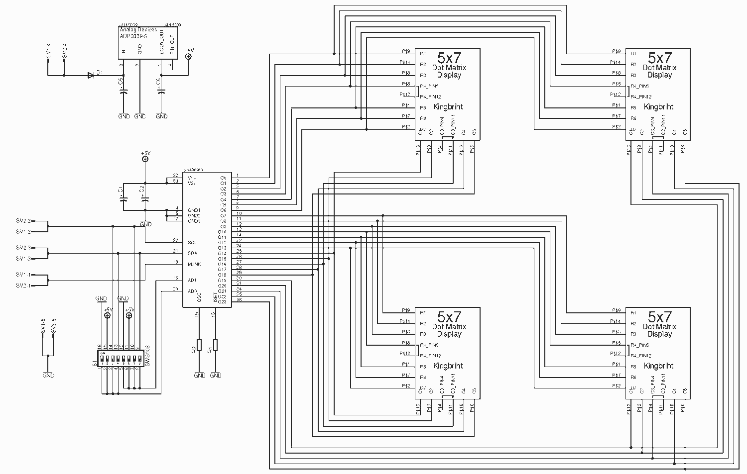
The MAX6953 from Dallas Maxim is a compact cathode-row display driver that interfaces a microprocessor (like PIC or AVR) to four 5x7 dot matrix LED displays through an I2C compatible serial interface. The chip includes some features that can...
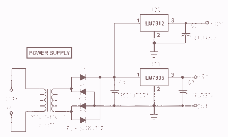
The power supply section is the important one. It should deliver constant output regulated power supply for successful working of the project. A 0-12V/500 mA transformer is used for this purpose. The primary of this transformer is connected in...
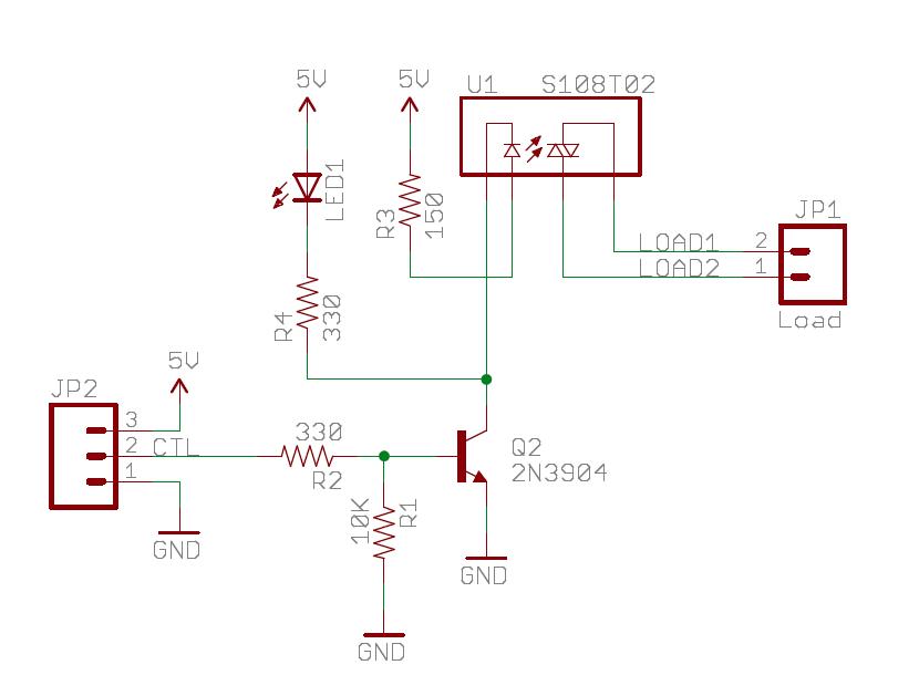
The Sparkfun Solid State Relay (SSR) Breakout Board operates similarly to a traditional relay but utilizes semiconductors for switching. It is powered by the mbed VU 5V supply and is compatible with any mbed digital output pin. The schematic...
The Atmel AVR series are very good microcontrollers with quite a rich instruction set, rich enough that lots of folks have good compilers for them so we don’t have to learn their assembler. A very rich compiler available is...