
8051 Development System Circuit Board 3
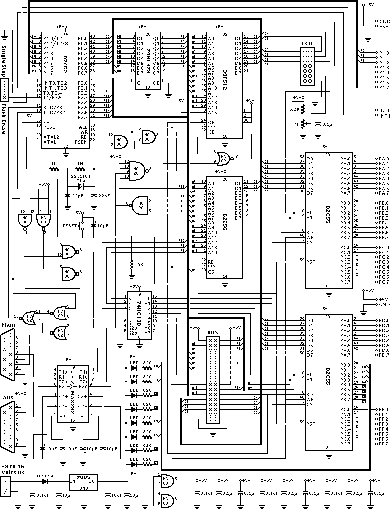
The schematic illustrates a well-structured design aimed at efficient communication between the microcontroller and various memory components. The unique address bus configuration allows for efficient wiring, reducing complexity in the layout. The use of the 74HC373 flip-flops facilitates the handling of multiple data lines without the need for extensive routing, as any of the identical flip-flops can be utilized interchangeably. The RAM and Flash ROM chips are seamlessly integrated into the system, allowing for flexible data storage and retrieval without concern for physical mapping, which is crucial for dynamic applications.
The MAX232 chip's role in converting TTL logic levels to RS-232 standards is critical for serial communication, and the choice of capacitor values provides flexibility while maintaining functionality. The design's attention to noise reduction through careful routing and decoupling strategies ensures reliable operation, especially in environments susceptible to interference.
The memory addressing scheme, utilizing NAND gates and the 74HC138 decoder, efficiently manages access to the RAM and Flash ROM, ensuring that the processor can communicate with the appropriate memory component based on the address signals. This method allows for organized memory access and peripheral management, a vital aspect of any embedded system.
Overall, the schematic represents a thoughtful integration of various components, balancing simplicity in construction with advanced functionality, suitable for a range of applications in electronics and embedded systems.This schematic is provided in the hope that it will be useful, but without any warranty, not even a warranty of merchantability or fitness for a particular purpose. The address bus in this schematic is connected in an unusual way, which is optimized for simpler point-to-point wiring and board layout.
For anyone building the board using wire-wrap o r hand soldered point to point construction, this wiring scheme makes for much less clutter in the wiring if the chips are positioned similarly to the layout on the printed circuit board. This unusual address bus wiring works. The 74HC373 chip (U2) is 8 identical flip-flops, so it does not matter which one is used for each line.
On the RAM (U3) and Flash ROM (U4) chips, all data that is stored in these chips is written by the 87C52 chip (U1), so it does not matter which physical location within the chip is mapped into each location within the CPU`s address space, because each read from these chips will return the same data that was written from a previous write. Some readers have felt that it`s "just not natural" to connect any other way than P0. 0-D0-Q0-A0, P0. 1-D1-Q1-A1, and so on, but it does indeed work. For a historic example, Woz used a very creative address bus connection scheme in the Apple ][ to automatically do DRAM refresh with his video refresh reads.
Because he arranged the address pins a certain unusual way, every video mode accessed each DRAM row several times per video refresh, so he didn`t need to add the cost and space of the usual DRAM refresh circuits (he interleaved video and cpu memory access, since the 6502 spends half its time not fetching anything). It works, and Apple sold millions of them! The MAX232 chip (U9) is shown with C3, C4, C5, and C6 as 1 µF, but the board is usually built with 10 µF capacitors (as shown in the parts list below).
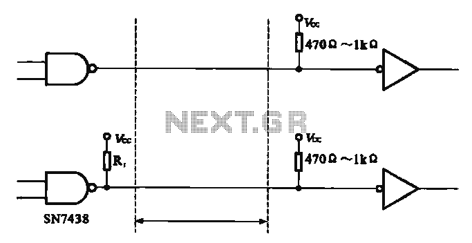
Either will work. C6 is connected to ground. In the sample circuit within the datasheet, it is connected to Vcc. Either connection will work. This connection causes charge-pump current flow through C8 and C10, but it avoids coupling the Vcc line to the V+ pin (high frequency digital switching noise, relative to ground, despite C11-C17). The V+ pin is ultimately connected via the MAX232 driver to the RS-232 cable. The basic idea is that some logic chips connect to the upper address bits and they assert on of the chip select signals, depending on what memory range the processor is accessing.
The A15 signal goes directly to the RAM, so the RAM gets selected for all addresses where A15 is low (0000 to 7FFF). A11 to A14 go to a 4-input NAND gate. That gate outputs low when all four signals are high, and its output is low in all other cases. That gate and the A15 signal go to the other 4-input NAND gate and to the 74HC138 chip. When A15 is high, and any of A11 to A14 are low, the other 4-input NAND gate drives the flash rom chip select low.
That means the flash rom is enabled from the range 8000 to F7FF. Those same two signals also go to the 74HC138 chip`s G1 and G2a inputs. The 74HC138 only drives one of its outputs low when G1 is high and when G2a is low. That means the 74HC138 chip drives one of its 8 signals in the range of F800 to FFFF. The three address inputs to the 74HC138 are connected to A8, A9 and A10, so that each of those signals corresponds to a 256 byte range. If you follow where each one goes, you`ll see they correspond to the memory map for the periperals. Most of the chips are designed to connect directly to the bus, so all that`s needed is to connect their address pins to the lower pins of the address bus, their data pins to the data bus, and their write and output enable pins to the WR and RD/PSEN signals.
All the chips see all those signals, but only the chip that gets a low signal on its chip select pin will communicate with the processor. All the other chips remain silent. The 8051 provides the address information before it asserts RD, WR or P 🔗 External reference
Related Circuits
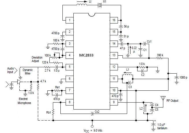
A simple FM transmitter circuit can be designed using the MC2833 integrated circuit, which is intended for cordless telephones and FM communication equipment. It features a microphone amplifier, a voltage-controlled oscillator, and two auxiliary transistors. The final output frequency...
This circuit design for a high-frequency waveform generator is highly beneficial for electronic experiments and designs. The circuit generates sine wave oscillations, but it can also be modified to produce triangle or square wave functions. The high-frequency waveform generator circuit...
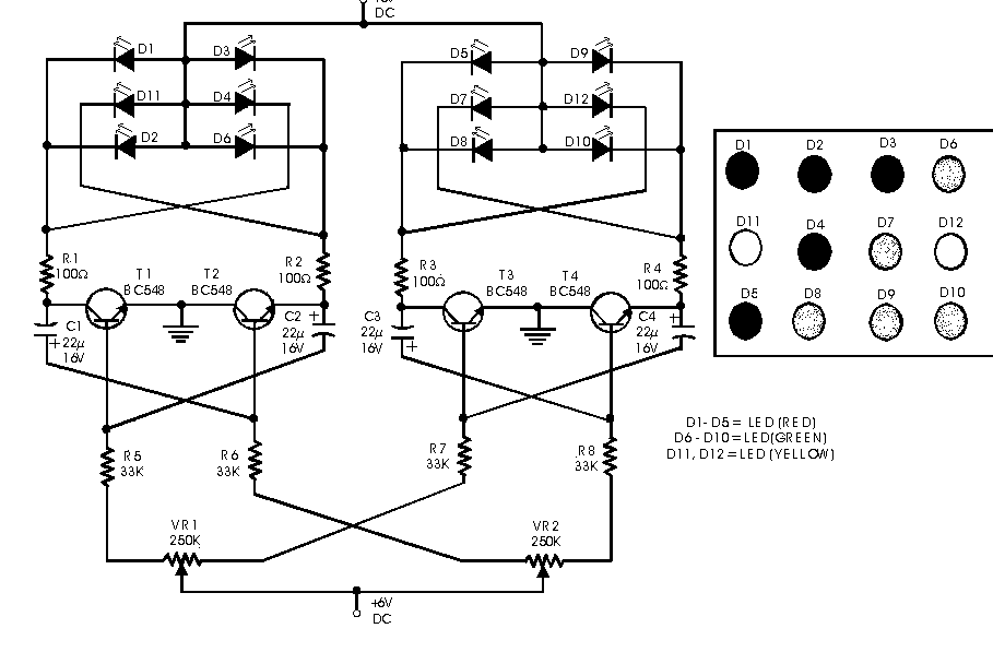
This circuit serves as a decorative element or indicator, featuring adjustable flashing or dancing speeds of LEDs and the ability to create various light patterns. It comprises two astable multivibrators; the first is constructed using transistors T1 and T2,...

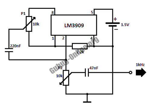
A 1-kHz gated oscillator with no long turn-on cycle is shown. R2, R3, and D1 preset the voltage on tuning capacitor C1 to a percentage of the supply voltage. The circuit described functions as a gated oscillator operating at a...
Examples of an OFDM modulation system. The graph illustrates the input data signal (.... --- Ol01100) and the data signal by the string. The input signal is separated into components such as "00", "ll", "10", "00", "01", and other...
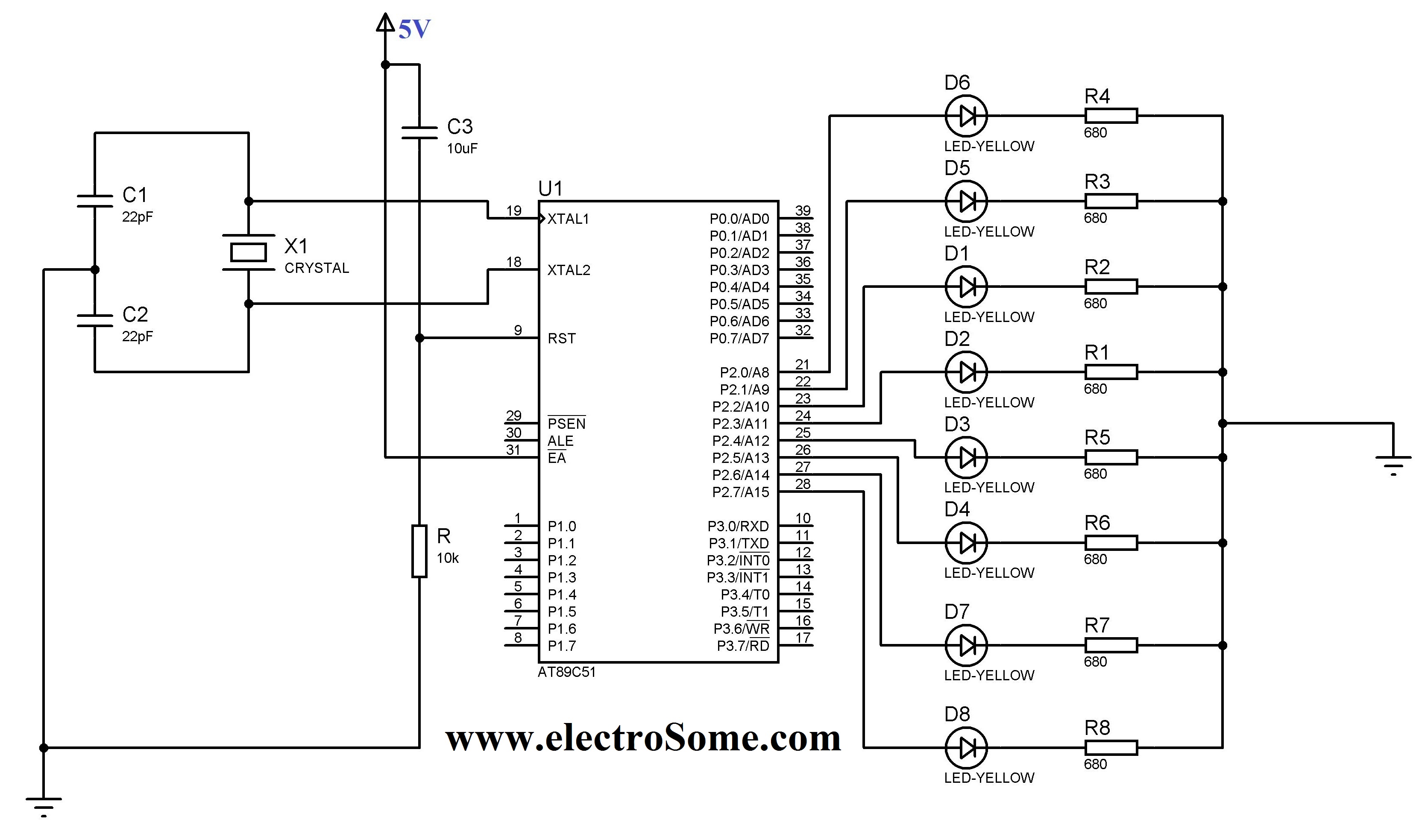
The 8051 controller is mask-programmable, meaning it is programmed during manufacturing and cannot be reprogrammed afterward. However, the AT89C51 microcontroller, a derivative of the 8051, is reprogrammable. This device includes a timer, a serial port interface, and interrupt control,...
Warning: include(partials/cookie-banner.php): Failed to open stream: Permission denied in /var/www/html/nextgr/view-circuit.php on line 713
Warning: include(): Failed opening 'partials/cookie-banner.php' for inclusion (include_path='.:/usr/share/php') in /var/www/html/nextgr/view-circuit.php on line 713