
9400 Selling Leads 9400 Datasheet PDF
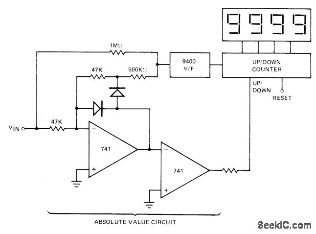
The absolute-value integrator circuit is designed to process analog signals by integrating the input voltage over time while maintaining a non-negative output. This is particularly useful in applications where it is necessary to analyze both positive and negative portions of a waveform without losing information due to the signal's polarity.
In this circuit, the input signal is fed into an integrator, which can be implemented using operational amplifiers (op-amps) configured for integration. The output of the integrator reflects the integral of the input voltage, effectively translating the input signal's area under the curve into a corresponding voltage level. To ensure that negative input voltages do not adversely affect the operation of the circuit, an absolute-value mechanism is employed. This can be accomplished using a combination of diodes and op-amps.
When the input signal is positive, the integrator counts up, reflecting the accumulation of positive voltage over time. Conversely, when the input signal turns negative, the absolute-value integrator allows the circuit to reverse the polarity of the negative voltage, effectively enabling the counter to count down. This dual counting mechanism results in the generation of negative frequencies, which can be particularly beneficial in various signal processing applications, such as in frequency modulation or in systems requiring phase detection.
The choice of diodes in this circuit is flexible, as long as they can handle the required forward current and reverse voltage. Standard silicon diodes are often sufficient, but Schottky diodes may be used for faster switching times if required by the application. The integration time constant can be adjusted by selecting appropriate resistor and capacitor values in the feedback loop of the op-amp, allowing for customization based on the desired response characteristics.
Overall, the absolute-value integrator circuit is a versatile tool in electronic signal processing, capable of transforming waveforms while preserving essential information about both positive and negative signal components.Absolute-value integrator circuit gives effect of generating negative frequencies when input signal is negative by making counter count up for positive voltage and count down for negative voltage. Diode types are not criticaL-M. O. Paiva, "Applications of the 9400 Voltage to Frequency Frequency to Voltage Converter, " Teledyne Semiconductor, Mounta
in View, CA, 1978, AN. 10, p 3. 🔗 External reference
Related Circuits
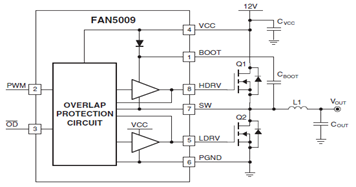
The schematic illustrates a typical application circuit for the FAN5009, a dual bootstrapped 12V high-frequency MOSFET driver. When integrated with a multi-phase PWM controller and power MOSFETs, it can form a complete core voltage regulator for microprocessors, as specified...
Ducati Haynes PDF Manual PDF Download. The Ducati Haynes manual is a comprehensive guide designed for Ducati motorcycle owners and enthusiasts. It provides detailed information on maintenance, repair, and troubleshooting for various Ducati models. The manual typically includes sections on...
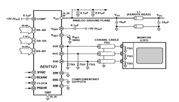
This digital-to-analog converter (DAC) integrated circuit is designed for optimal noise performance, minimizing both radiated and conducted noise. A recommended connection diagram for the ADV7123 is depicted in the following schematic diagram. According to the ADV7123 datasheet, this device...

The schematic diagram below illustrates a 5V/1A Step-Down Switching Regulator utilizing the LM2524D Regulating Pulse Width Modulator (PWM). Additional parameters, PC board layout, stuffing diagram, and more information can be found in the LM2524D datasheet. The circuit design features the...
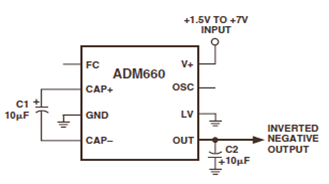
The ADM660 is a charge-pump voltage converter that can either invert the input supply voltage or double it. The schematic below depicts the ADM660 Voltage Inverter Circuit Configuration Diagram. This inverting schematic is ideal for generating a negative rail...
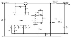
The circuit illustrates a TL494 pulse width modulated step-down converter schematic. This circuit allows for testing of line regulation, load regulation, output ripple, short circuit current, and efficiency under various input voltage conditions. A detailed table of these tests...
Warning: include(partials/cookie-banner.php): Failed to open stream: Permission denied in /var/www/html/nextgr/view-circuit.php on line 713
Warning: include(): Failed opening 'partials/cookie-banner.php' for inclusion (include_path='.:/usr/share/php') in /var/www/html/nextgr/view-circuit.php on line 713