
A Low-Frequency Crystal Controlled Oscillator
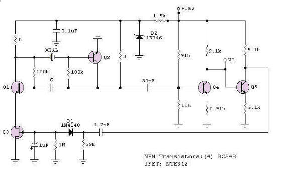
The described low-frequency sine wave oscillator circuit is designed to provide precise control and reliable operation across a specified frequency range. The use of bipolar transistors in the oscillator and amplifier stages ensures that the circuit remains cost-effective while delivering high performance. The modified astable multivibrator configuration allows for automatic adjustment of the loop gain, ensuring stable oscillation without manual intervention. The incorporation of a JFET for loop-gain control is particularly advantageous, as it allows for fine-tuning of the circuit's response to external conditions, such as temperature changes and power supply variations.
The isolation provided by Q4 is critical for maintaining signal integrity, preventing any non-linear effects from the rectifier D1 from impacting the output waveform. This careful design consideration is essential for applications requiring high fidelity, especially in laboratory settings where precision is paramount. Additionally, the feedback mechanism that adjusts the gate voltage of Q3 plays a vital role in maintaining consistent output amplitude, which is crucial for applications that rely on stable signal generation.
The selection of resistor values based on frequency is a practical approach to accommodate the varying characteristics of low-frequency quartz crystals, ensuring optimal performance across the specified range. The circuit's ability to maintain low distortion levels below 0.1 percent further enhances its suitability for precision applications. The inclusion of a zener diode to stabilize the power supply further contributes to the circuit's robustness, making it a reliable choice for RF engineers seeking to test low-frequency quartz crystal units effectively.The RF engineer sometimes has to look for an instrument that will check a low frequency quartz crystal unit reliably and rapidly. This is a difficult piece of equipment to find and the engineer often has to consult an electronic circuits handbook for the schematic of a circuit that will perform the task.
Unfortunately, there aren`t many such circu its in the technical literature currently available, and when found, they don`t always work as expected. A circuit that has been found to work at full satisfaction in the frequency range from 10 kHz to 500 kHz is illustrated in Figure 1.
This is a schematic of a low frequency sine wave oscillator featuring low distortion, wideband operation and crystal control. The circuit, originally developed for laboratory use, employs low cost AF bipolar transistors for the oscillator and amplifier sections and a JFET for loop-gain control.
Operation of the oscillator in the 10 kHz to 500 kHz frequency range has been found to be excellent, while measured distortion is kept under 0. 1 percent. Q1, Q2 and associated circuitry form a modified astable multivibrator in which the loop gain is automatically adjusted to the threshold of oscillation by means of field effect transistor Q3.
Q4 linearly amplifies the signal present at the collector of Q2 and isolates the oscillator section of the circuit from the output. This stage features wideband operation and delivers a clean 2. 5 Volt amplitude sine wave into a resistive load greater than or equal to 20 kohms. The stage comprising Q5 has a voltage gain of 1 and its sole purpose is to isolate the non-linear effects of rectifier D1 from the output.
Transistor Q4 also amplifies the minor changes in amplitude of the oscillator`s waveform due to temperature effects and/or power supply variations, so a magnified version of the perturbance is fedback to rectifier D1 producing a corresponding change in Q3`s gate voltage. This action modifies the FET`s drain-source resistance and hence adjusts the loop gain to a new value slightly above unity, just enough to maintain a constant amplitude in the output.
Figure 2 shows optimum values for capacitor C according to the crystal`s resonant frequency. Extra gain is needed from transistors Q1 and Q2 at frequencies below 40 kHz. This is due to the fact that low frequency crystals exhibit large values of series resistance, affecting loop gain (Table 1 compares typical values of series resistance for low frequency units). According to what has been stated, resistor R is made 10 kohms for frequencies under 40 kHz. Above this value, 1 kohm will do. 3) Due to the dynamic action of the JFET the output level is almost insensitive to power supply variations.
The 3. 3 Volt zener diode further enhances this result. 🔗 External reference
Related Circuits
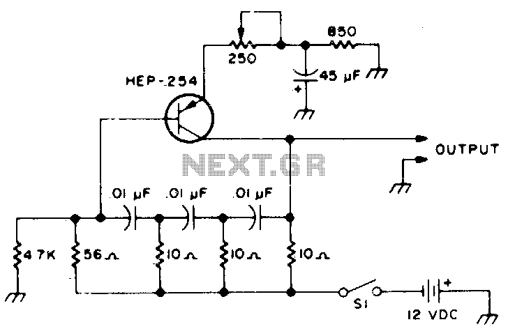
The following transistors may be used: HEP-254, OC-2, SK-3004, AT30H. To increase the frequency, decrease the value of the capacitors in the ladder network. The transistors listed, HEP-254, OC-2, SK-3004, and AT30H, can serve various roles in electronic circuits, particularly...
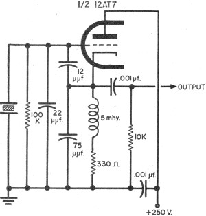
To update the fundamental oscillator circuits, simply replace the transistors with tubes. Alternatively, if one owns a vintage vacuum tube radio, it may be of interest to learn about historical practices. In general, the foundational principles of electronic circuits...
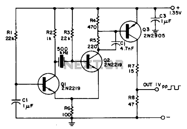
The circuit is powered by a single 1.35 V mercury cell and provides a 1 V square-wave output. The crystal acts as a tuned circuit between transistors Q1 and Q2, which are connected in a common-emitter configuration. Positive feedback...

Each step will result in a self-functional unit. By the end of this process, it will be possible to link the steps together into a powerful FM transmitter. This section will explain the main controlling unit for the FM...
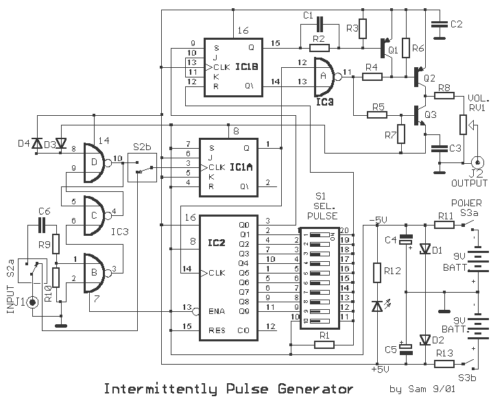
The generators of square pulses are used in a lot of applications, including the adjustment of conditions of entry in digital circuits and the control of acoustic frequency amplifiers. This circuit is a generator that produces, in combination with...
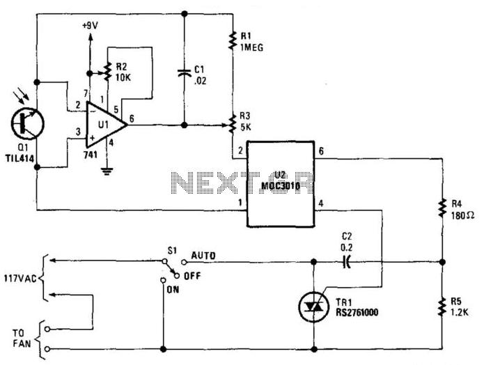
Q1 senses infrared radiation from heat sources, which causes U1 to switch on, activating optocoupler U1 and triggering TRIAC TR1. This controls a fan. The TRIAC can be sourced from Radio Shack or a 200-V, 6-A unit (C106B) can...
Warning: include(partials/cookie-banner.php): Failed to open stream: Permission denied in /var/www/html/nextgr/view-circuit.php on line 713
Warning: include(): Failed opening 'partials/cookie-banner.php' for inclusion (include_path='.:/usr/share/php') in /var/www/html/nextgr/view-circuit.php on line 713