
Calculate magnification input resistance and output resistance circuit

This circuit is designed to calculate the magnification, input resistance, and output resistance of a given electronic system. The magnification refers to the ratio of the output signal to the input signal, which is a crucial parameter in amplifying circuits. Input resistance is the resistance seen by the input signal, while output resistance is the resistance encountered by the load connected to the output.
To analyze the circuit, a typical operational amplifier (op-amp) configuration can be employed. In a non-inverting amplifier setup, the input signal is applied to the non-inverting terminal of the op-amp. The feedback network, usually consisting of resistors, determines the gain (or magnification) of the circuit. The gain can be calculated using the formula:
\[ \text{Gain (A)} = 1 + \frac{R_f}{R_i} \]
where \( R_f \) is the feedback resistor and \( R_i \) is the resistor connected to the inverting terminal.
The input resistance of the circuit can be approximated by the resistor \( R_i \) in the non-inverting configuration, as the op-amp itself has a very high input resistance, thus minimally affecting the input signal. Therefore, the input resistance \( R_{in} \) can be expressed as:
\[ R_{in} = R_i \]
For the output resistance, in an ideal op-amp, the output resistance is considered to be zero. However, in practical applications, the output resistance can be affected by the load connected to the output. The output resistance \( R_{out} \) can be calculated based on the configuration and any load resistances connected.
In summary, this circuit enables the calculation of magnification, input resistance, and output resistance through the use of an op-amp in a non-inverting configuration, providing essential parameters for evaluating the performance of electronic amplifiers in various applications. Calculate magnification, input resistance and output resistance circuit
Related Circuits

The Zener diode functions as an avalanche rectifier in reverse bias mode, connected to the input circuit of a wideband RF amplifier. The noise is amplified and subsequently applied to the cascade wideband amplifier, utilizing transistors Q2 and Q3. The...
Electrical signals travel along the neurons in the brain and body, continuously transmitting information throughout the complex system. Without these signals, the body would function like a plant, with different parts unaware of each other's conditions, making animal life...
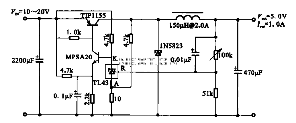
The 5V regulator circuit is designed to convert a DC input voltage ranging from 10V to 20V into a stable 5V output. This circuit features low power consumption and high efficiency. The 5V regulator circuit typically employs a linear voltage...
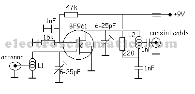
A simple and cost-effective TV antenna amplifier circuit is constructed using the BF961, a dual-gate N-channel MOSFET, which serves as the input and mixer stages. The described TV antenna amplifier circuit utilizes the BF961 dual-gate N-channel MOSFET due to its...
Energy-saving lamps are categorized into self-ballasted compact types and single-ended structures. They can also be classified based on appearance into various forms such as double-tube, four-tube, six-tube types, and others. The lifespan of energy-saving lamps is approximately ten times...
This amplifier circuit is designed to enhance TV signals in the UHF range. It employs a low-noise transistor, providing an amplification of 10 to 15 dB within the frequency spectrum of 400 MHz to 850 MHz. It is crucial...