
A simple DDS for 136kHz
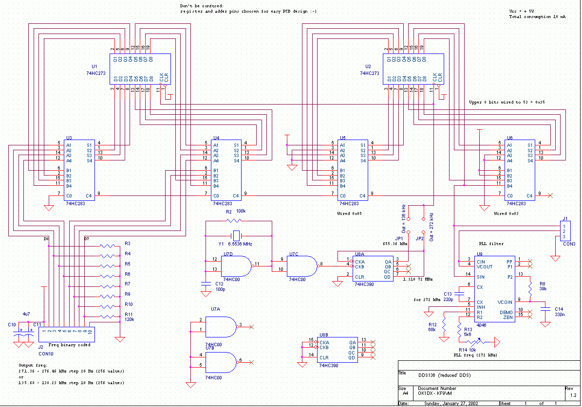
The circuit employs hex switches for user input, where each switch provides a binary input to the system. The arrangement allows for a straightforward interface for selecting values, with the common pin connected to a +5V supply, ensuring that the switches can operate correctly. The modification of the oscillator circuit highlights the importance of component selection and values in achieving reliable operation. By increasing the resistance of R2 to 1 Meg-Ohm and adding a capacitor for stability, the oscillator can be fine-tuned to work effectively with the chosen crystal.
Decoupling the VCO is critical in preventing noise from affecting its performance. The recommendation to use a regulated 5V supply emphasizes the need for stable power to ensure the proper function of sensitive components like the 4046 chip. The tolerance of other chips for up to 6V indicates a design consideration for flexibility in power supply options.
The inclusion of a buffer stage to shift the output voltage to 12V is necessary for compatibility with the G3YXM transmitter. The use of a common-emitter NPN transistor configuration is a standard approach in level-shifting applications, providing adequate gain and output drive capability. The resistor values chosen for the base and collector ensure that the transistor operates within its linear region, allowing for effective signal transmission over a meter of coaxial cable, which is crucial for maintaining signal integrity in RF applications.The Hex switches are connected to J2 as follows: pin 1=common of both switches (+5V) 2=LSB up to 5=MSB of first switch. Then 6=LSB of second switch up to 9 which is MSB. I modified the oscillator slightly to get my cheap Farnell crystal to start reliably (Philips 74HC00 chip).
Increase R2 to 1 Meg-Ohm add another C of about 200pF from pins 9, 10, 11 to earth. Ensure you decouple the VCO (4046) chip properly and choose a 5V regulator with a slightly high output (it MUST be fed from a regulated supply), it didn`t seem to like 4. 9V! The other chips will stand up to 6V. You will need a buffer stage to level-shift up to 12V if you want to drive the G3YXM TX with it. I used a single common-emitter NPN stage; 10k from input to base, 4k7 from base to ground, 1k from collector to 12V, emitter grounded.
The output comes from the collector. This isn`t great but it will drive down a metre of coax! 🔗 External reference
Related Circuits
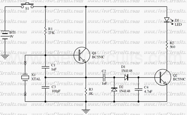
This is a simple XTal tester circuit. T1 and XTal have formed an oscillator. C1 and C2 are voltage divider for oscillator. if the XTal is safe, the oscillator will work well and its output voltage will be rectified...
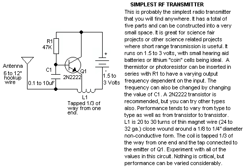
This schematic represents a tone transmitter. When using sufficiently small resistor values, it generates a tone. A resistive microphone (such as a carbon microphone) can be placed in parallel with or replace the resistor, allowing modulation of the tone...
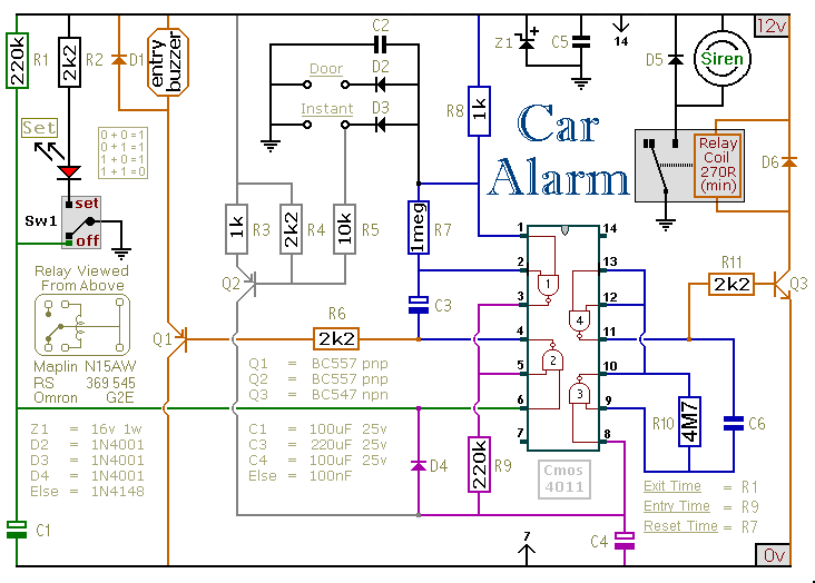
This circuit includes automatic exit and entry delays, an optional instant alarm zone, an optional intermittent siren output, and an automatic reset feature. By incorporating external relays, it is possible to immobilize the vehicle and activate the lights. For...

A 555 IC is configured to function as a Schmitt trigger. Inputs above and below the threshold level will turn the circuit on and off, producing a square wave output. The 555 timer integrated circuit (IC) is a versatile device...

The 555 IC is configured in an astable mode, producing a frequency that remains constant and is independent of the duty cycle. The total resistance (Rcharge + Rdischarge, considering the diode) is fixed at 22 kΩ, yielding a frequency...

This circuit is designed to charge between one and twelve NiCd cells using a car battery. With switch S1 set to the normal position, it is capable of charging up to six cells. The circuit operates by utilizing a car...