
A watchdog circuit diagram
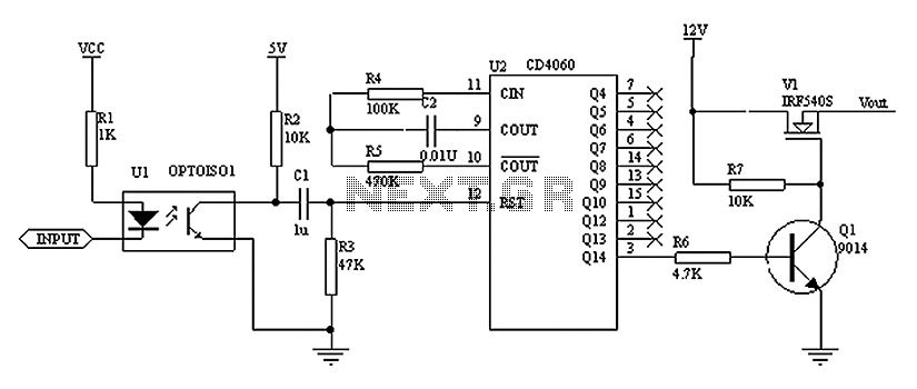
The described circuit utilizes a CD4060 integrated circuit, which functions as a frequency divider and oscillator. This device is pivotal in generating the timing signals necessary for the operation of the NMOS transistor and the LED. The reset pulse is essential for initializing the CD4060, ensuring that the output states are correctly set before the circuit begins its primary function.
The timing components, including resistors R2 and R3 and capacitor C1, are configured to create a delay that allows sufficient time for the system to stabilize. The choice of these components directly affects the duration of the reset pulse. A longer time constant can be achieved by increasing the values of R2 and C1, thus providing an extended initialization period for the processor circuitry.
The NMOS transistor serves a dual purpose: controlling the LED and acting as a switch that provides power to the processor. When the reset pulse is active, it ensures that the NMOS transistor remains in the conductive state, allowing current to flow through the LED, which indicates that the circuit is powered and operational.
Despite its advantages, the circuit's reliance on a wide pulse width can limit its applications. The design must ensure that the pulse width is adequate to trigger the NMOS transistor consistently; otherwise, the circuit may fail to operate as intended. Therefore, careful consideration must be given to the pulse generation mechanism to ensure reliable performance.
Overall, this circuit design is an effective solution for applications requiring a delayed initialization sequence, provided that the pulse width requirements are met. Its low cost and simplicity make it a suitable choice for various electronic projects.As Figure: when the operation of the circuit as long as the timing of the reset pulse to the CD4060, we can guarantee the state ended in Q1, so that the NMOS transistor control led in the on state power to the processor circuitry. The advantage of this circuit is that the timing of the time can be relatively long, a few minutes no problem, it can take a long time to those who have enough time to initialize the system for initialization. Pulse trigger the dogs, when the power through R2, C1, R3 an automatic reset pulse to the counter to ensure that there is an output Vout.
Circuit costs low.The biggest drawback of this circuit is that the dogs require a relatively wide pulse.
Related Circuits
The power supply has been simplified. Power transformers and rectifiers have been omitted, and some components from the MOSFET voltage regulator circuits have been removed, including 1N5242 zener diodes between the source and gate and 10k resistors in series...

An AC-coupled unity gain voltage follower operating on a single supply is illustrated. The voltage divider network consisting of resistors R1 and R2 provides a DC voltage equal to half the supply voltage to the non-inverting input of the...
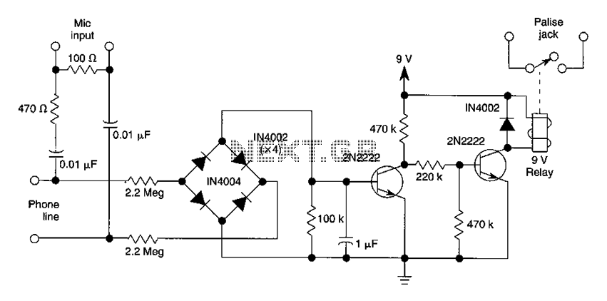
The DC voltage present on the telephone line typically ranges from 45 to 50V when on-hook and drops to approximately 6V when off-hook. This condition activates a step-down circuit relay, which in turn controls a tape recorder. Audio input...
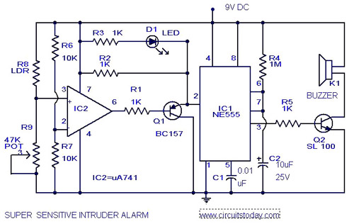
The circuit diagram illustrates an ultra-sensitive intruder alarm. The mere shadow of an intruder passing within a few meters of the circuit is sufficient to activate the alarm. In this setup, the IC2 uA741 is configured as a sensitive...
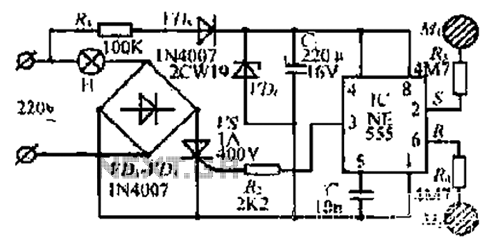
220V AC by Ri buck, Diao. C1 chain ferry flood ear, shouted for the regulator to 12V make C collapse. The film hand touch under ridicule the MT electrode films, clutter body. More: induction signal sent by See Cutting...
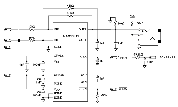
Incorporate a straightforward, economical jack-sensing circuit (JACKSENSE) into a DirectDrive automotive headphone amplifier to detect when headphones are plugged into the audio jack. The implementation of a jack-sensing circuit (JACKSENSE) in a DirectDrive automotive headphone amplifier is designed to enhance...