
AC time delay circuit with 555
The timer circuit described operates within a standard electrical system to control a light bulb without requiring modifications to existing wiring. It connects in parallel with an existing switch or button, enabling the bulb to remain illuminated for a duration after the switch is turned off. The compact design allows installation within a standard electrical box, ensuring minimal disruption to existing setups.
The timer is activated by a voltage drop, which can occur during power interruptions or fluctuations, such as those caused by storms or electrical work. This feature is particularly beneficial in areas with unstable power supply. The timer circuit utilizes a Triac for switching, which operates effectively under both closed and open conditions.
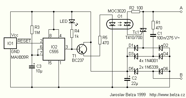
The circuit design incorporates a bridge rectifier (D1, D2, D5, D6) to manage power supply to the bulb and the timer. Zener diodes (D5, D6) stabilize the output voltage, maintaining consistent performance. The circuit includes a reactive power flow through resistor R1 and capacitor C1 to manage idle conditions, while diodes D3 to D6 assist in voltage stabilization.
An LED indicator is included to signal when the timer is ready for operation. A resistor (R4) is included to manage idle load, and if an indication is not required, it can be bypassed with a jumper. The circuit's timing is primarily controlled by the resistor R3 and capacitor C3, which define the duration the bulb remains lit after activation.
The optotriac (O1) and triac (TC1) form the core of the switching mechanism, ensuring safe operation across different voltage potentials. The circuit is designed to handle a maximum load of approximately 100 W, with provisions for higher loads through alternative configurations. The integrated circuit MAX809R serves as the timer control, with its threshold voltage set for reliable operation.
The assembly of the circuit board is straightforward, with specific components laid out to facilitate ease of soldering and assembly. The design is intended for users with basic electronic skills, providing clear instructions for setup and operation. Overall, the timer circuit enhances the functionality of standard light switches, offering convenience and efficiency in lighting control.Described timer to participate in the current circuit switch - bulb without any modification of existing pipelines. Connect the timer is in Figure 1 The time switch has only two outlets, which is connected in parallel to the button (Fig.
1a) or switch (Fig. 1b). If you use the button works as a classical staircase circuit switch. Connect a timer switch in parallel to the original, we will extend bulb shines as the time required to leave the room. Dimensions of the timer are so small that it can be installed into standard electrical box under the original power switch.
The wiring does not need to change anything, there is no need nor any assistant conductor. The timer is triggered by voltage drop. Switch closes when the interrupt for a moment the power supply which can happen even when a storm or manipulations in the substation. In places where the network is "soft" power matters and executive appliances such as vacuum cleaner. Timer scheme is in Figure 2 Resolve power circuit was the hardest nut of the whole structure. The timer must be operated in both closed, and unfastened Triac. If no voltage is present, eg when the terminals A and B shorted out the button, the power is restored after running the timer circuit. If the triac is closed, current passes through the bulb (see Figure 1) to supply and triac and through the bridge rectifier diodes D1, D2, D5 and D6.
In place of the D5 and D6 are used in Zener diodes with voltage 5.6 V Zener diode turns in stabilizing the momentary polarity. Voltage drop between terminals A and B is about 7 to 8 in which the brightness of bulbs virtually no impact.
The idle circuit is the reactive power flow, passing through the resistor R1 and capacitor C1. The streamlining is now used diodes D3 to D6. The output voltage is stabilized Zenerovými diodes, as well as in the previous case. The filter capacitor C2 is intentionally very low capacity to respond timer for a short press. Zener diodes limit the maximum switching capacity. Power Zener Diode 1N5339 meet the load 398 W. Then, however, each Zener diode loses power almost 5 watts, which is not in a small space dissipate electrical box. Therefore, I recommend not to use a larger ratio than the burden of about 100 W. For higher performance should be possible to replace the D5 and D6 conventional rectifier diodes and output voltage stabilization regulator connected in parallel to C2.
In idle status LED lights to indicate ready timer. Emitting diode with R4 is also necessary to idle load circuit. After switching button and shorting pins A and B, see Figure 1, the capacitor C2 is rapidly discharged below the threshold voltage IO1. Because his own collection IO1 and IO2 is very small (in the implementation of CMOS) is required mentioned resting load.
If you do not need an indication, do not use LEDs, but you must replace it with a jumper. Resistor R4 then magnify the 2.2 to 3.3 kW. When running MKO is on the IO2 pin 3 voltage near the positive supply voltage. Resistor R5 and a current through the optocoupler triac is closed. Participation was accompanied by a transistor T1, which enhances the power output of the optocoupler IO2. The switching part is made optotriakem O1 and triac TC1. Using optotriaku was necessary because the triac is in a different potential than the timer circuit. Rated current input optocoupler LED is 20 mA. So great power for switching is not available. The entire load current passes through the first switch C1 is about 7 mA. Resistor R5 is current limited to about 6 mA. I tested several optotriak? from different manufacturers and only one needed for a full switch current of about 7 mA, meet others.
Incomplete closing affects not only the less bright bulb, but the buzzing district. If the timer did not work properly, I was looking for a mistake here. Construction and recovery The circuit board for a timer and layout of components in Figure 3 and 4 If you do not want you to count, you can choose to delay decisive components in the table. The album will be filled by components such as last Solder IO1 and IO2. IO1 is soldered to the board of the joints. Capacitor C1 is placed horizontally next to the printed circuit boards. Implementation of the plate is shown in the accompanying photo. R1, R5 470 W D1 to D4 1N4007 R2 100 W D5, D6 1N5339B, ZD 5.6 V / 5 V R3 1-10 MW, see text T1 BC237 (BC548, etc.) R4 1 kW IO1 MAX809R C1 NF/275 100 V, CFAC IO2 C555 (KS555, TS555, etc) C2 ?F/16 22 V electrolytic O1 MOC3020 C3 10-47 ?F/16 V, see text TC1 T410/700 PCB LED any low-power Integrated circuit MAX809R.
Finished switch connecting terminals A and B, parallel to the button or switch. Swap pin has no effect on the operation. The recovery is very simple - if you make a mistake, switch on the first working connection. While working, keep the necessary precautions, the device is electrically connected to the network. For this reason, design for beginners. The timing circuit is used in known circuit 555, this time in a CMOS implementation, which involved a monostable flip-flop. The trigger circuit is used MKO MAX809R. The connection type is used MAX809R the threshold voltage of 2.63 V. Switching time is determined by resistor R3 and capacitor C3, connected to terminals 6 and 7, IO2 and can be calculated by the formula t = 1.1 R3 C3 [a, MW, uF].
🔗 External reference
Related Circuits
A 12V battery charging circuit is presented, featuring a straightforward diagram for a rectifier. The lead-acid trickle charger circuit is detailed along with its rectifier. The 12V battery charging circuit is designed to charge lead-acid batteries using a trickle charging...

The circuit diagram and detailed explanation of a simple aircraft radio circuit are provided below. The simple aircraft radio circuit typically consists of several key components that work together to facilitate communication between the aircraft and ground stations or other...
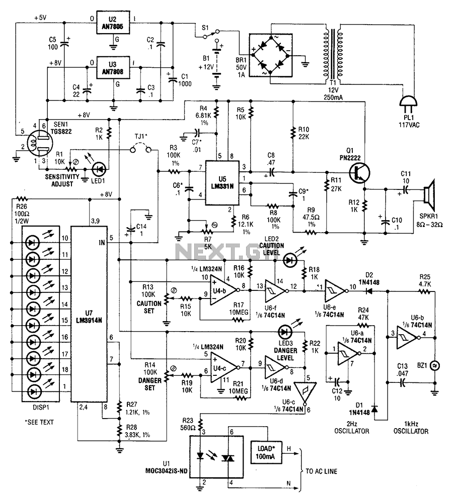
A gas sensor (from Allegro Electronics, Cornwall Bridge, CT06754 Ts GS823) activates in the presence of explosive gas. U5 functions as a voltage-to-frequency converter, with the sensor producing a frequency that is proportional to conductance. The output frequency varies...

After acquiring a large 3-phase variable transformer (variac), there was an unexpected issue with it tripping circuit breakers at random when plugged in. Interestingly, the tripping occurred on different phases and seldom affected all three simultaneously. Resetting the breakers...
The amplifier circuit utilizing the STK4050 integrated circuit (IC) is known for its robustness and high quality. This article presents a 200-watt power amplifier circuit based on the STK4050. The circuit features an advanced auto wiring diagram with color-coded...

VDI, VD2, C3, and C4 form a simple half-wave rectifier capacitor step-down regulator circuit. This circuit can output approximately 12V DC voltage after power is applied across C3, which is utilized for the time base circuit. Additionally, the time...