
Active Antenna With Gain
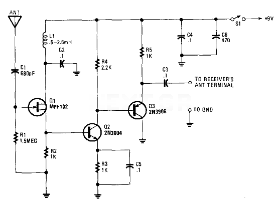
The schematic for the described signal booster includes three primary transistors: Q1, Q2, and Q3. Q1 is typically a field-effect transistor (FET) that acts as the initial RF signal amplifier. The direct coupling of the source terminal of Q1 to the base of Q2 ensures that the amplified signal from Q1 is efficiently transferred to the voltage amplifier stage, Q2. This configuration is critical for maintaining signal integrity and minimizing losses.
Transistor Q2 is configured to amplify the RF signal further, and its output is then directly coupled to Q3. The emitter-follower configuration of Q3 allows for a high input impedance and a low output impedance, which is essential for effectively driving the input of the subsequent circuitry in the receiver. This isolation provided by Q3 prevents loading effects that could otherwise degrade the performance of the preceding amplification stages.
The inductor L1 plays a vital role in filtering out any noise from the power supply, ensuring that only the desired RF signal is amplified. The choice of an RF choke between 0.5 to 2.5 mH is optimal for this application, as it balances the need for effective filtering while maintaining bandwidth.
Resistor R2 is crucial for setting the bias point of Q2. A bias voltage of approximately 2 V is necessary for optimal operation of Q2. Should the bias voltage drop below this level, increasing R2 to 1.5 kΩ will help restore the proper biasing conditions. This adjustment is important for maintaining the linearity and efficiency of the amplifier.
Capacitor C1 is used to adjust the lower frequency response of the circuit. Increasing its value to 0.002 µF allows the circuit to effectively amplify signals below 100 kHz, thus expanding its operational frequency range.
The antenna design, specified as a short pull-up type with a length between 42 inches and 86 inches, is suitable for this application as it balances size and performance, allowing for effective signal reception across the specified frequency range.
Overall, this signal booster design exemplifies a straightforward yet effective approach to RF amplification, utilizing fundamental electronic components to achieve desirable performance metrics in a compact form. The signal booster, built around a few transistors and support components, offers an RF gain of about 12 to 18 dB (from about 100 kHz to over 30 MHz). The RF signal is direct-coupled from Ql"s source terminal to the base of Q2, which is configured as a voltage amplifier. The output of Q2 is then direct-coupled to the base of Q3 (configured as an emitter-follower amplifier).
Transistor Q3 is used to match and isolate the gain stage from the receiver"s RF-input circuitry. Inductor LI is used to keep any power source noise from reaching the FET (Ql) and any value of RF choke from 0.5 to 2.5 mH will do. The value of R2 sets the Q2 bias at about 2 V. If the voltage is less than 2 V, increase the value of R2 to 1.5 KOhmhm. To go below 100 kHz (to the bottom of the RF spectrum), increase the value of CI to 0.002uf. The antenna is a short pull-up type (42" to 86" long). 🔗 External reference
Related Circuits

This wideband antenna preamplifier has a gain of approximately 20 dB from 40 to 860 MHz, covering the entire VHF, FM, commercial, and UHF bands. A phantom power supply delivers DC power to the preamplifier through the coaxial cable...
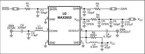
This application note presents alternate RF matching networks for the MAX2653 SiGe LNA, tuned for the GPS band (1575 MHz center frequency). Performance metrics (supply current, forward gain, noise figure, IIP3, reverse isolation, and input/output return loss) for both...
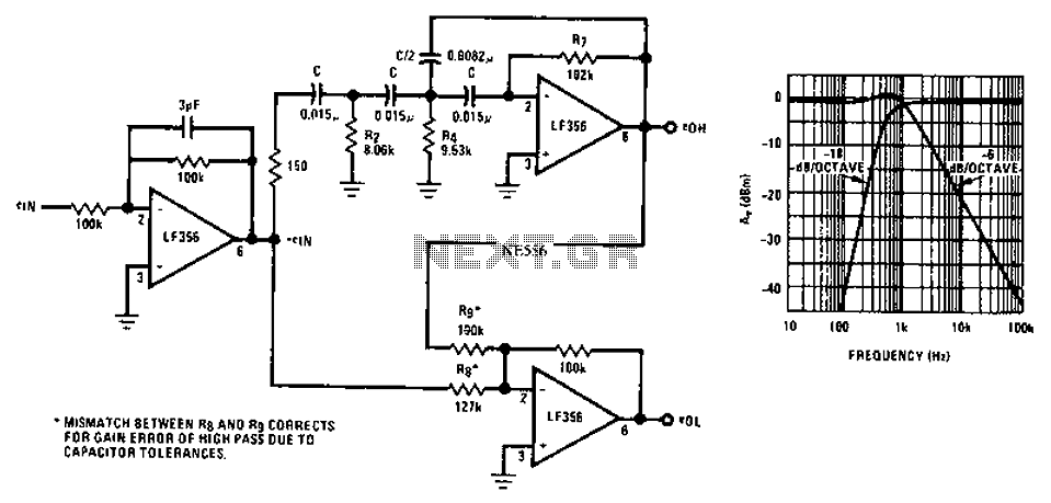
Asymmetric third-order Butterworth active crossover network circuit diagram. The asymmetric third-order Butterworth active crossover network is a sophisticated circuit designed to split an audio signal into two separate frequency bands, typically for use in multi-way speaker systems. This type of...
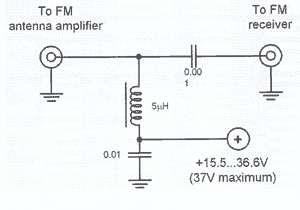
This technique eliminates the need for an additional cable to power the FM antenna amplifier. The RF signal and the DC current that supplies the amplifier utilize the same cable simultaneously. An FM antenna booster circuit diagram can be...

This filter circuit, which utilizes the LM1458 or a similar operational amplifier, has a frequency response ranging from 300 Hz to 3.4 kHz, exhibiting a roll-off of 12 dB per octave outside the passband. Section A serves as the...
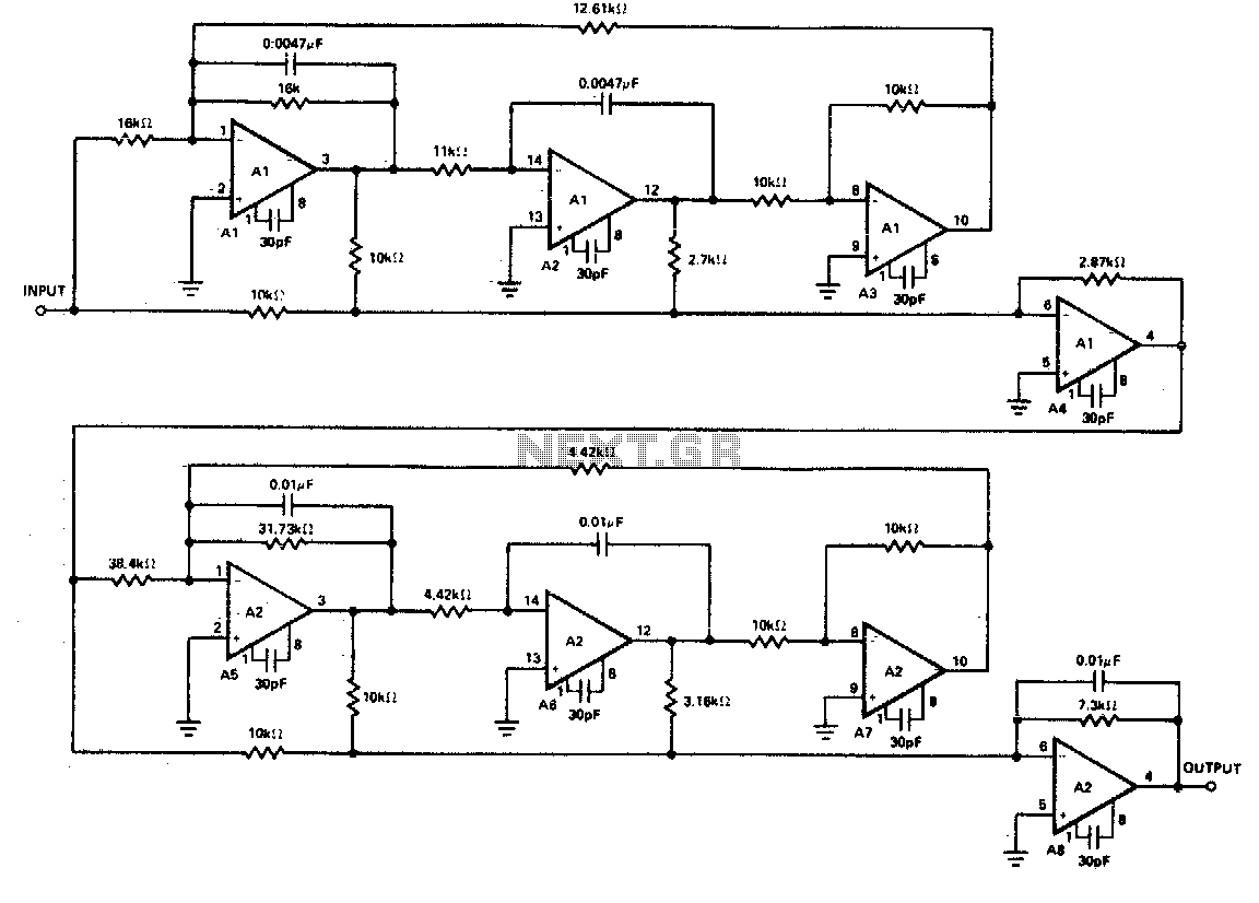
The realization of a type 03 receive filter is achieved using eight OP-08 operational amplifiers. The response curve indicates that the requirement for greater than 30 dB attenuation in the stop band has been satisfied. Furthermore, the noise performance...