
FM Antenna Amplifier Circuit

This FM antenna amplifier design effectively integrates the power supply and RF signal transmission through a single coaxial cable, enhancing efficiency while reducing installation complexity. The active amplifier circuit, placed near the antenna, is crucial for boosting weak RF signals. The use of MOSFETs in this circuit design is significant, as these components help prevent intermodulation distortion, which can degrade signal quality.
The circuit's configuration includes LC filters that serve to isolate the RF signal from the power supply, ensuring that only the intended signals are amplified while preventing unwanted feedback that could interfere with performance. The amplifier's gain of 25 to 30 dB is suitable for improving signal strength, making it ideal for applications where signal clarity is paramount.
The power supply circuit is designed to provide a stable DC voltage to the amplifier, with specific voltage ranges that must be adhered to for optimal performance. The measurements taken during testing—such as the DC voltage in the cable and the voltage at the collector of T5—are critical for verifying that the circuit operates within the desired parameters. The specified voltage levels at various points in the circuit, such as the emitter of T2 and the resistor R4, are indicators of proper functionality. Monitoring these values ensures that the MOSFETs are operating efficiently, which is essential for maintaining the integrity of the RF signal and the overall performance of the antenna system.
Overall, this circuit design represents a sophisticated approach to enhancing FM signal reception while minimizing the complexity of installation and operation.With this technique, an extra cable to power the fm antenna amplifier is unnecessary. The RF signal and the DC current supplying the amplifier use the cable simultaneously. Check another FM antenna booster circuit diagram. The RF signal is however prevented by LC filters from flowing into the power supply. The amplifier works with either 50 ohm or 75 ohm antenna. It has a gain of 25 30 dB. MOSFETs are used to avoid the problem of crossmodulation or intermodulation. The circuit is divided into two parts. The first part is the active aplifier circuit which is normally installed very near the antenna. The second part is the power supply circuit which supplies current to the amplifier through the coax cable. After the fm antenna amplifier circuit is constructed, the power supply should be connected to it. You must then test the DC voltage in the cable. This must be between 15. 5 and 36. 6 volts. Then test the voltage between T5 collector and ground while adjusting the supply voltage. It must move from 3 to 24 volts. The emitter of T2 should be approx. 11. 4 volts. If the voltage at R4 is between 0. 7 and 2 volts, then the MOSFET is functioning properly. 🔗 External reference
Related Circuits
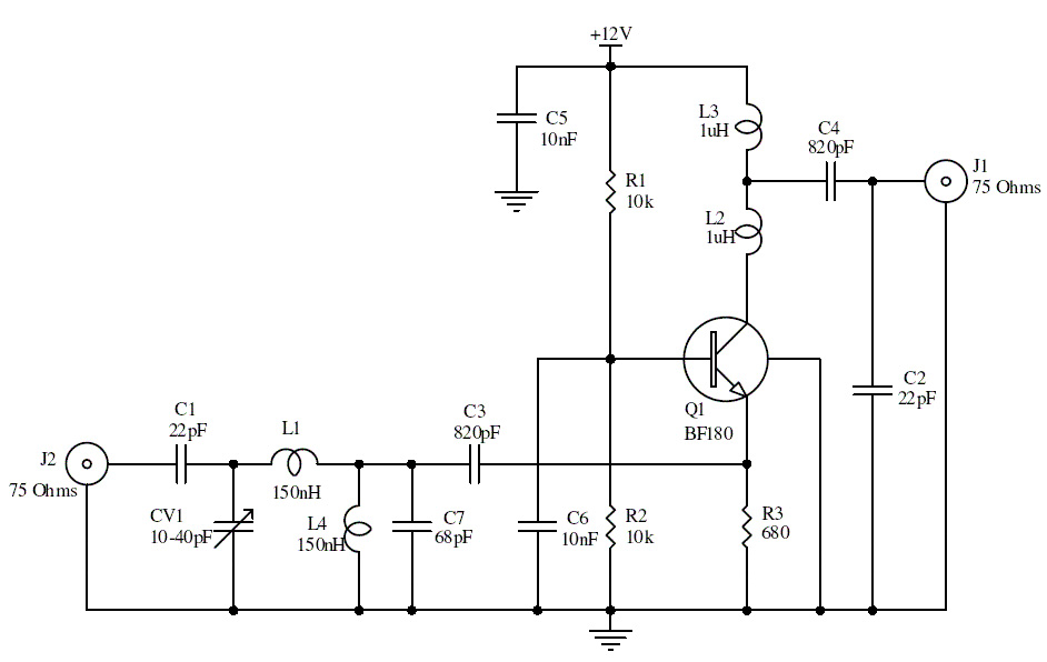
This is a UHF band TV antenna preamplifier circuit with a gain of 15 dB. It is designed using the BF180 UHF transistor. The input stage consists of a band-pass filter implemented with components C1, CV1, L1, L4, C7,...
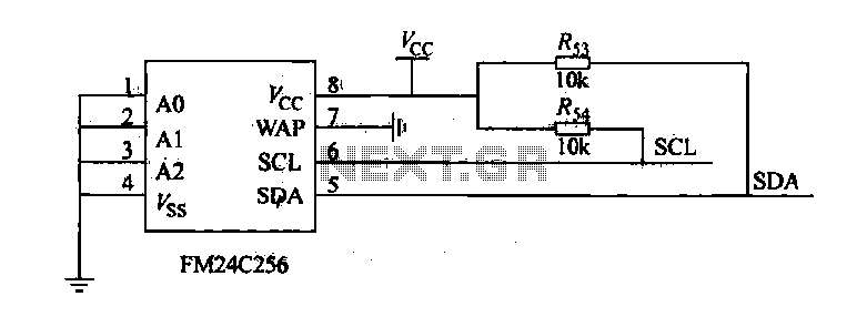
The FM24C256 is utilized as a slave interface circuit in an I2C bus configuration, with the address format specified in Table 27-3. The address pins A2, A1, and A0 are set to low; however, for extended storage capacity, adjustments...
The YD9088 is a bipolar integrated circuit designed for use in mono portable and pocket radios. It is advantageous when minimizing peripheral components, which should be of small dimensions and low cost, is a priority. The circuit incorporates a...
TDA2050 audio amplifier circuit diagram. The circuit incorporates environmental protection, where the output signal travels through connecting cables and the speaker’s network. In this case, the reactance of the circuit section connected to pin 4 of the chip is...
In all the houses exist the bells in the door. All want, they have the possibility of being possible to change the intensity, the tone of sound. With this circuit we have this possibility. With the materials round the...

The RF amplifier Q3 connects to diodes D1 to D4 within the mixer. Transistors Q1 and Q2, through transformers T1 and T2, facilitate the injection of liquid oxygen at 10 MHz for diodes D1, operational amplifier U1A, and U1B....