
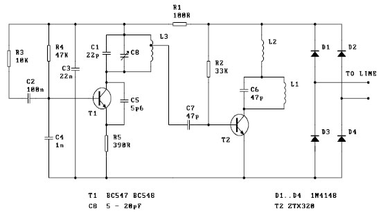
Active FM Antenna Booster circuit PCB

The described circuit involves an FM antenna booster that utilizes two coils, L1 and L2. Coil L1 serves as the primary inductive element, while coil L2, which has only three turns, is used for coupling and signal enhancement. The tapping of coil L2 at the first turn from the ground lead indicates a design choice aimed at optimizing the inductance and maximizing signal reception.
The transistor 2SC2570 is a crucial component in this circuit, functioning as an amplifier. Its pin configuration must be accurately followed to ensure proper functionality. The transistor operates within its specified parameters to amplify the signals received by the antenna.
Adjustable trimmers, designated as VC1 and VC2, are incorporated into the circuit to allow for fine-tuning of the input and output impedance. Proper adjustment of these trimmers is essential for achieving maximum gain, which enhances the overall performance of the antenna booster. The adjustment process typically involves monitoring the output signal strength while varying the trimmer settings to find the optimal configuration.
The schematic should include clear representations of the coil windings, the transistor connections, and the trimmer locations, ensuring that all components are correctly aligned for effective operation. This design is particularly useful in environments with weak signal reception, providing an improved signal strength for FM radio applications.It is tapped at the first turn from ground lead side. Coil L2 is similar to L1, but has only three turns. Pin configuration of transistor 2SC2570 is shown in the fm antenna booster schematic. Adjust input/output trimmers (VC1/VC2) f or maximum gain. 🔗 External reference
Related Circuits
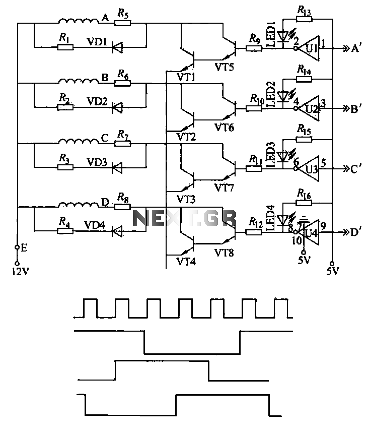
This machine utilizes the FD-CAS-923 1-stepper motor control experiment board with a 4-phase stepper motor to avoid its schematic shown in Figure 4-42a. The JK1 cop 40 core flat cable connector allows for signal arrangements compatible with EICE51 simulation...
The 7th overtone of 18 MHz (17m) is 144 MHz (2m) directly within the CW region. Icarus is a high-altitude balloon (HAB) project funded by advertising revenue, which has successfully launched numerous balloons that captured impressive photographs. Robert Harrison...
This FM spy telephone circuit is connected in series with the phone line. When there is a signal on the wires, this transmitter will radiate airwaves through the wires. This FM spy telephone circuit operates by integrating with the existing...
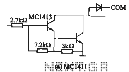
The MC1411 series is a Darlington driver with a compact, reliable internal structure. It is particularly suited for high-voltage applications, functioning effectively as a high-voltage peripheral driver. This driver can directly control relays, lights, and other loads. It is...
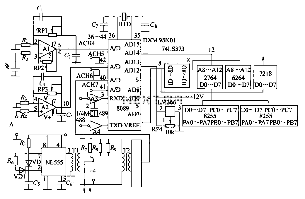
Direct measurement circuit for soil content, assessing various parameters such as moisture, salinity, nitrogen, and pH to enhance soil quality for diverse agricultural crops. This electronic measuring circuit facilitates rapid and accurate testing of soil conditions and informs fertilization...
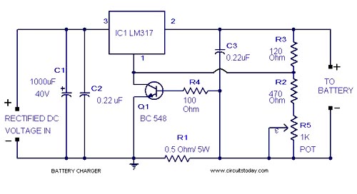
A simple lead-acid battery charger circuit with a diagram and schematic using the IC LM317, which provides the correct battery charging voltage. This lead-acid battery charger should be supplied with an input of 18 volts to the IC. The lead-acid...