
ADC In An FPGA
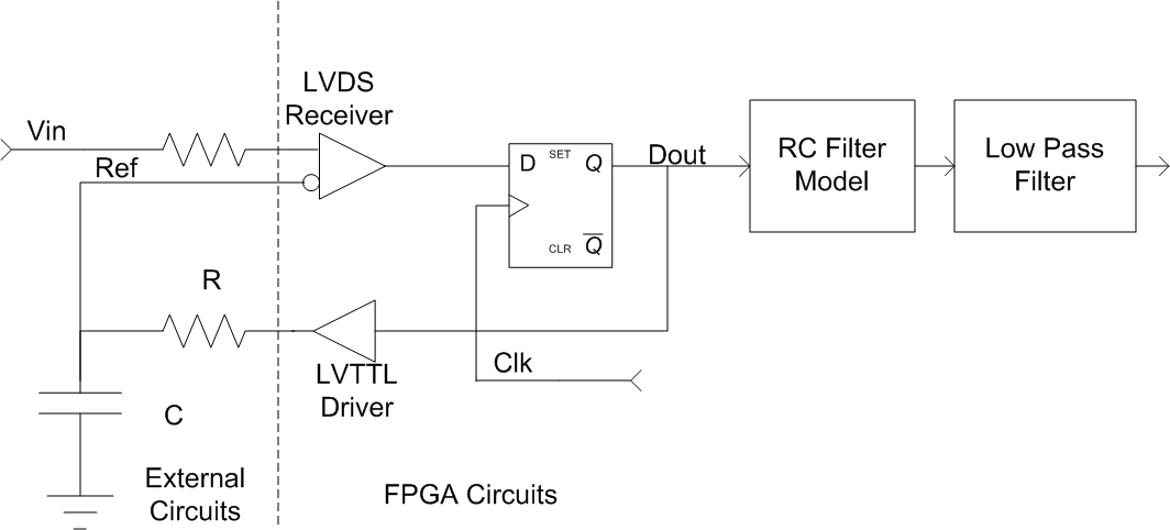
The circuit design focuses on integrating Analog-to-Digital Converters (ADCs) with Field Programmable Gate Arrays (FPGAs) to create a sophisticated electrical system capable of processing analog signals with high precision. The ADC serves as the interface that converts continuous analog signals into discrete digital values, which can then be manipulated by the FPGA.
In this schematic, the ADC is connected to the FPGA via a high-speed serial interface, ensuring rapid data transfer. The choice of ADC is critical; it must have a suitable sampling rate and resolution to meet the application requirements. For instance, a 12-bit ADC with a sampling rate of 1 MSPS (Million Samples Per Second) would be appropriate for many applications requiring moderate precision and speed.
The FPGA, programmed with a specific logic design, processes the digital signals received from the ADC. The FPGA may include various digital signal processing (DSP) blocks that can filter, amplify, or otherwise modify the input signals based on the desired functionality. The flexibility of FPGAs allows for reconfiguration, enabling the design to adapt to different signal processing tasks without the need for hardware changes.
Power supply circuits are also a crucial aspect of the design, ensuring that both the ADC and FPGA receive stable voltage levels. Decoupling capacitors should be placed close to the power pins of the components to minimize noise and provide a clean power source. Additionally, a proper grounding scheme must be implemented to reduce interference and improve overall system performance.
In summary, the integration of ADCs and FPGAs in this electrical design provides a powerful solution for real-time signal processing applications. The ability to customize the FPGA logic and the precision of the ADC make this combination suitable for a wide range of technical applications, from telecommunications to industrial automation.Geek Alert! What follows is very technical. It involves ADC`s, FPGA`s, and sophisticated electrical design. If this doesn`t sound like you then you can safely skip the rest of this blog post. EDIT: Part 2 of this series is up. Read it here, when you`re done with Part 1, of course. I`ve always had this. 🔗 External reference
Related Circuits

ZTEX USB-FPGA Boards require three different voltages: 1.2V, 2.5V-2.6V, and 3.3V, which must be supplied externally. This can be achieved using Power Supply Modules, Experimental Boards, or a user-specific design. To facilitate development in the latter scenario, three reference...
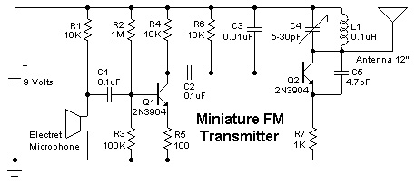
Construct a simple mini FM transmitter. This engaging project demonstrates how to create a mini broadcasting transmitter capable of transmitting an audio signal up to a quarter mile to any FM receiver. It is straightforward to assemble and offers...
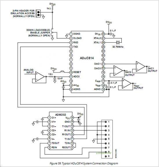
The ADUC816 is a complete smart transducer front-end that integrates two high-resolution sigma-delta ADCs, an 8-bit microcontroller unit (MCU), and program/data Flash EEPROM memory on a single chip. This low-power device accepts low-level signals directly from a transducer. The...
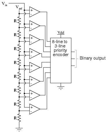
Also known as the parallel A/D converter, this circuit is the simplest to understand. It consists of a series of comparators, each comparing the input signal to a unique reference voltage. The outputs of the comparators connect to the...
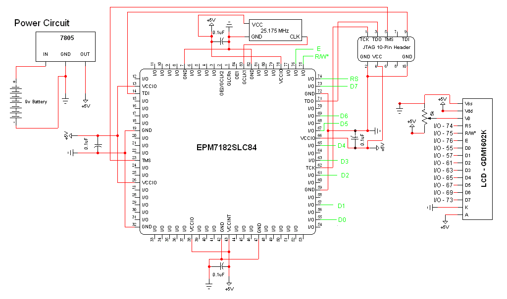
The schematic for this project is a modified version of the CPLD development board schematic. Several new components have been added for this project, and the completed schematic is presented below. The primary components in the schematic include the...
This article discusses practical techniques for incorporating "correctness by design" in DDR2 interfaces from a Signal Integrity (SI) perspective, utilizing the current generation of available design tools. It analyzes common DDR2 design errors and the trade-offs between various popular...